Deep-Ultraviolet and Vacuum-Ultraviolet Lasers: Multidimensional Expansion of Application Frontiers
The technological innovation and application expansion of deep-ultraviolet (DUV) and vacuum-ultraviolet (VUV) lasers exhibit a deeply integrated development trend, where synergistic advancements in performance, functionality, and cost control continuously reshape the technical frontiers of semiconductors, new energy, and quantum science. The following systematically integrates the expansion logic and practical cases of these two laser types in application scenarios from the core pathways of technological innovation:
I. Three-dimensional Breakthroughs in Technological Innovation and In-depth Application Penetration
1. Performance Dimension: From "Parameter Upgrades" to "Scenario Adaptation"
Deep-Ultraviolet Lasers:
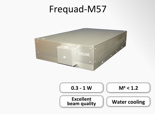
High Power & Stability: OXIDE's QCW 266nm laser has increased output power to over 6W with wavelength stability of ±0.1nm. In semiconductor EUV lithography auxiliary processing, it enables silicon wafer etching precision at the 3nm node, reducing defect rates to below 0.5%. In biomedicine, this performance supports single-molecule fluorescence imaging with a resolution 突破 (breaking through) 30nm, facilitating real-time tracking of β-amyloid plaques as markers for Alzheimer's disease.
Long-life Crystal Technology: Ultra-high-purity BBO crystals (lifespan >5,000 hours) enable continuous cutting of perovskite layers in HJT photovoltaic cell mass production, improving processing efficiency by 50% compared to traditional lasers and achieving a yield rate of 98.5%.
Vacuum-Ultraviolet Lasers:
Integration & Low Noise: The PEV series reduces ARPES equipment debugging time from 2 weeks to 8 hours through fully integrated optical units. In solid-state battery electrolyte research, it enables real-time monitoring of electron energy spectrum changes during Li⁺ migration, accelerating the development of high-conductivity materials. The space charge effect suppression technology in PEV-H achieves an excitation precision of 0.1nm on graphene surfaces, providing critical data for quantum tunneling device interface design.
2. Functionality Dimension: From "Single Light Source" to "Comprehensive Solutions"
Deep-Ultraviolet Lasers:
Full-band Spectrum Coverage: The 213nm–266nm wavelength range adapts to diverse material absorption characteristics. For example, 236.5nm laser has an ozone absorption cross-section of 1.5×10⁻¹⁹cm², driving the miniaturization of portable ozone monitors with a detection precision of 0.1ppb. The 257.5nm laser replaces argon ion lasers, reducing semiconductor lithography equipment maintenance costs by 60%.
Energy Efficiency Innovation: The integration of quantum cascade lasers and fiber technology increases energy conversion efficiency to 35%. In OLED screen cutting for consumer electronics, it achieves edge roughness below 1μm while reducing power consumption by 40%, pushing flexible screen mass production yield rates beyond 95%.
Vacuum-Ultraviolet Lasers:
Expanded Photon Energy: Future breakthroughs in 15eV (83nm) photon energy will directly excite surface state electrons in topological insulators, enabling observation of electron transport trajectories in the "quantum anomalous Hall effect" for quantum computer chip R&D and providing experimental foundations for spintronic device design.
3. Cost Dimension: From "High-end Monopoly" to "Scalable Affordability"
Deep-Ultraviolet Lasers:
Domestic Substitution & Scaling: Enterprises like Han's Laser have reduced the cost of 266nm lasers by 40% through all-solid-state architectures, increasing their penetration rate in university research from 25% in 2023 to 50% in 2025. Undergraduates can use this equipment for Raman spectroscopy experiments. In consumer electronics, cost reductions have enabled deep-ultraviolet laser processing of TWS headphone casings with roughness <0.5μm, lowering mass production costs by 30%.
Vacuum-Ultraviolet Lasers:
Modular Design for Cost Reduction: Pre-integrated optical modules have decreased PEV series production costs by 25%, allowing small and medium-sized material enterprises to purchase the equipment for surface electron state detection of nano-catalysts. This shortens the R&D cycle from 12 to 6 months, accelerating the commercialization of new environmental catalysts.
II. Closed-loop Drive Model of Technology-Application Integration
| Technological Innovation Direction | Breakthroughs in DUV Laser Applications | Breakthroughs in VUV Laser Applications | Driving Logic |
| High power/wavelength stability | 3nm chip lithography, single-molecule detection | Real-time electronic structure analysis of high-temperature superconducting materials | Precision requirements drive performance upgrades |
| Full-band spectrum/energy efficiency | High-efficiency processing of photovoltaic cells, ozone monitoring | Transitional band research for soft X-ray photoelectron spectroscopy (SXPS) | Material properties match spectral expansion |
| Integration/cost control | Popularization of precision processing in consumer electronics, (sinking) of research equipment to universities | Reduced R&D costs for small and medium-sized enterprises in material science | Market scale drives industrial cost reduction |
III. Future Trends in Technology-Application Integration
1.Integration with Quantum Optics: Combining DUV lasers with quantum dot light sources will enable single-photon-level precise excitation, pushing the manipulation accuracy of quantum bits in quantum computing to over 99.9%.
2.Breakthroughs in New Crystal Materials: The R&D of nitride deep-ultraviolet crystals (e.g., AlN) is expected to expand laser wavelengths to 157nm, applying to light source pretreatment for extreme ultraviolet lithography.
3.Cross-disciplinary Application Ecosystem: Integrating VUV lasers with in-situ electron microscopy will enable simultaneous observation of material electronic structures and morphological changes at the nanoscale, providing "dynamic maps" for research on new energy battery interface failure mechanisms.
Conclusion: Technological innovation in DUV and VUV lasers is not isolated parameter optimization but a bidirectional evolution of "scenarios defining technology and technology reshaping scenarios," deeply coupled with demands from semiconductors, quantum science, new energy, and other fields. In the future, with interdisciplinary innovation in photonics and materials science, these two laser types will play core roles in more "bottleneck" technological fields (e.g., EUV lithography light sources, quantum device R&D), driving collaborative breakthroughs in high-end manufacturing and fundamental scientific research.
For more information on our OXIDE Deep-UV Single Frequency Lasers, please click here.
 English
 Français
 Deutsch
 euskara
 Русский язык
 Italiano
 Português
 Nederlands
 Polski
 Greek
Greek Lietuva
 Türkçe
 日本語
日本語 한어
한어 中文
中文 தாமில்
 فارسی
فارسی हिंदी
हिंदी Tiếng Việt
 ภาษาไทย
 Pilipino
 Indonesia
 தாமில்
