 English
 Français
 Deutsch
 euskara
 Русский язык
 Italiano
 Português
 Nederlands
 Polski
 Greek
Greek Lietuva
 Türkçe
 日本語
日本語 한어
한어 中文
中文 தாமில்
 فارسی
فارسی हिंदी
हिंदी Tiếng Việt
 ภาษาไทย
 Pilipino
 Indonesia
 தாமில்

OXIDE Deep Ultraviolet Quasi-Continuous Wave (QCW) 266nm Laser: A High-Performance UV Laser Solution
1. Product Overview
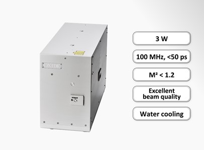
The OXIDE Deep Ultraviolet Quasi-Continuous Wave (QCW) 266nm Laser is an innovative laser product developed for users seeking higher output power than Continuous Wave (CW) lasers. Its core advantage lies in achieving low-peak-power pulses through a 100MHz high repetition frequency, which enhances power while significantly reducing damage to optical components and samples—approaching the damage level of CW lasers. Relying on OXIDE's over 20 years of technical expertise in high-performance nonlinear optical crystals and experience in minimizing Deep Ultraviolet (DUV) damage in CW single-frequency lasers, this product becomes a highly innovative and reliable 266nm high-power laser solution.
2. Core Technical Features
Ultra-High Purity BBO Crystal
Utilizes OXIDE proprietary BBO crystals, enabling the system to operate stably at 3W average power for over 5,000 hours.
The low-attenuation characteristics of the crystal ensure long-term high beam quality and stable output, providing a reliable guarantee for precision applications.
High-Reliability Fiber Amplification Technology
Constructs a stable high-power infrared light source through proprietary component technology, combined with a two-step wavelength conversion technique to achieve stable 266nm laser output, breaking through the power and stability bottlenecks of traditional UV lasers.
Low Power Consumption Design
The efficient wavelength conversion laser system keeps power consumption below <450W, significantly reducing energy consumption compared to similar high-power lasers while balancing performance and energy efficiency.
Exceptional Beam Quality
The beam quality factor M²<1.2 is close to the fundamental mode Gaussian beam, meeting the strict requirements for beam focusing accuracy in micron-level processing and precision detection.
3. Typical Application Scenarios
Semiconductor Manufacturing: Suitable for lithography equipment, wafer defect inspection, and other processes, leveraging the high-resolution characteristics of the deep ultraviolet band to achieve nanometer-scale pattern processing and precision inspection.
Spectral Analysis: Provides a stable UV excitation light source for Raman Spectroscopy and Photoluminescence detection, enhancing the sensitivity and accuracy of trace substance analysis.
Nano Laser Machining: Supports direct writing of nanoscale structures and micro-nano device manufacturing. Its low-damage characteristics are suitable for fine processing scenarios such as flexible electronics and biomedical sensors.
4. Analytical Overview of Deep Ultraviolet Laser Application Fields
4.1 Application Field Overview
Deep ultraviolet lasers (wavelength range typically 100-280nm) exhibit irreplaceable advantages in precision manufacturing, scientific research, life sciences, and other fields due to the high photon energy and high spatial resolution brought by their short wavelengths. The application value is analyzed from four core fields below:
4.2 Core Application Scenarios
Semiconductor and Microelectronics Industry
Lithography Technology: Assists Extreme Ultraviolet (EUV) lithography in advanced processes (such as below 7nm nodes) to achieve high-precision transfer of circuit patterns, breaking through the resolution limits of traditional optical lithography.
Wafer Inspection: Detects nanoscale defects (such as particle contamination and film defects) on wafer surfaces through Laser-Induced Fluorescence (LIF) or scattering imaging technology to ensure chip yield.
Packaging and Microprocessing: Used for cutting glass/ceramic substrates and through-hole processing in semiconductor packaging, as well as three-dimensional structure engraving of MEMS devices, with a processing accuracy of up to sub-micron level.
Optoelectronics and Precision Optics
Fiber Device Processing: Achieves precise modulation of the refractive index of the fiber core through deep ultraviolet laser exposure during the preparation of Fiber Bragg Gratings (FBGs), used for wavelength filtering and sensing in communication networks.
Optical Component Coating: Repairs nanoscale coating defects in optical lenses, lithography machine mirrors, and other components through Laser-Induced Chemical Vapor Deposition (LCVD) technology to achieve atomic-level film deposition.
LiDAR Component Manufacturing: Processes deep ultraviolet anti-reflective coatings for infrared optical components to improve the optical coupling efficiency of autonomous driving sensors.
Life Sciences and Medical Research
Single-Cell Analysis: Uses 266nm laser Ultraviolet-Induced Fluorescence (UVIF) technology to label and image biomolecules such as nucleic acids and proteins within single cells with a resolution of below 100nm.
Photodynamic Therapy (PDT): Activates photosensitizers through deep ultraviolet lasers to target and destroy cancer cells, avoiding damage to healthy tissues by traditional radiotherapy, suitable for local treatments of skin cancer and ophthalmic tumors.
Biochip Preparation: Removes photoprotective groups during the in-situ synthesis of DNA microarray chips to achieve precise arrangement of high-density biological probes.
Materials Science and Nanotechnology
Two-Dimensional Material Etching: Performs atomic-level etching on two-dimensional materials such as graphene and molybdenum disulfide (MoS₂) to fabricate prototype nanodevices such as single-electron transistors.
Metamaterial Fabrication: Constructs sub-wavelength-scale metamaterial structures (such as photonic crystals and metasurfaces) through two-photon polymerization technology by utilizing the nonlinear absorption of photosensitive resins induced by deep ultraviolet lasers.
Surface Functionalization Treatment: Initiates photochemical reactions on polymer and metal surfaces to generate nanoscale trenches or hydroxyl groups, enhancing material adhesion, hydrophilicity, or biocompatibility.
4.3 Application Compatibility of OXIDE 266nm Laser
The OXIDE deep ultraviolet QCW 266nm laser perfectly matches the stringent requirements of the above fields with its low-damage (100MHz high repetition frequency reduces thermal effects), high-stability (BBO crystal operates stably for 5,000 hours), and high-beam-quality (M²<1.2) characteristics:
Enables non-destructive rapid scanning of wafer surface defects in semiconductor inspection;
Supports the combination of femtosecond-level pulses and precision focusing in nano-machining to achieve mass production of nanowire and nanopore arrays;
Its <0.1nm linewidth characteristic meets the high-resolution excitation requirements for narrow-band fluorescent substances in spectral analysis.
4.4 Future Technology Trends
With the breakthrough of semiconductor processes to the 3nm node and the innovation of biological single-molecule detection technologies, deep ultraviolet lasers are developing towards higher power (such as the 6W output of the OXIDE prototype), shorter pulse widths (<50ps), and intelligent control. Technological innovations by enterprises like OXIDE will continuously promote the transition of deep ultraviolet lasers from laboratories to large-scale industrial applications, making them core enabling technologies of the Fourth Industrial Revolution.
For more information on our OXIDE Deep-UV QCW 266nm Lasers, please click here.