 English
 Français
 Deutsch
 euskara
 Русский язык
 Italiano
 Português
 Nederlands
 Polski
 Greek
Greek Lietuva
 Türkçe
 日本語
日本語 한어
한어 中文
中文 தாமில்
 فارسی
فارسی हिंदी
हिंदी Tiếng Việt
 ภาษาไทย
 Pilipino
 Indonesia
 தாமில்
Send us a message
CLOSE
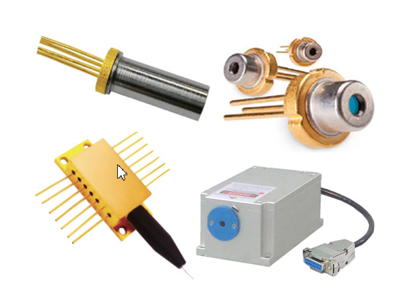
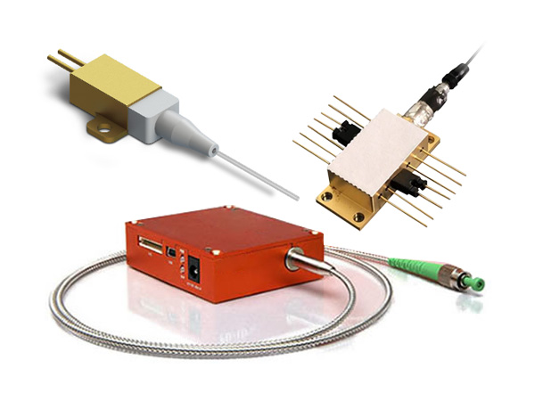
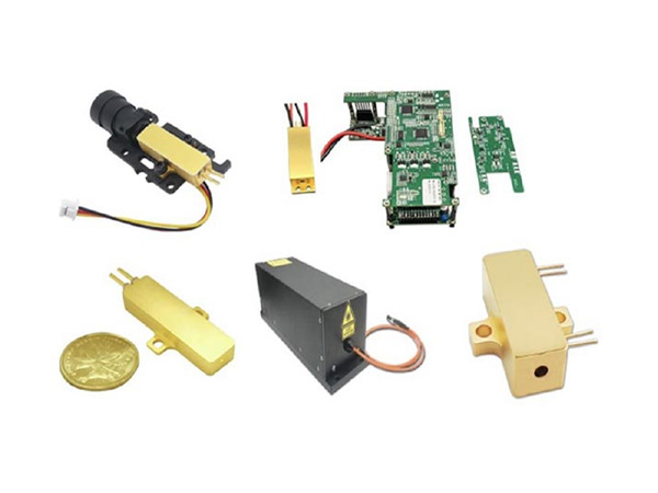


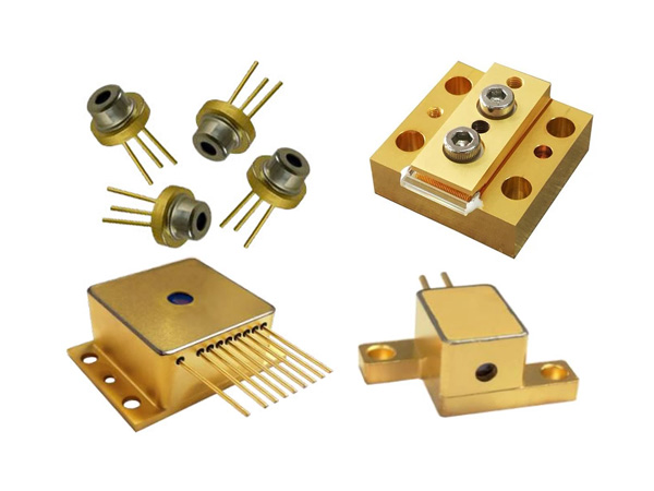
We offer a broad range of DFB lasers in the C-band and L-band on 50 or 100 GHz channel spacing as well as at 1310 nm, 1064 nm, and other custom wavelengths. Power level options include 40–100 mW out of the fiber for high power 14-pin lasers and 10-18mW options for high bandwidth 7-pin configurations. Distributed feedback lasers (DFB lasers) simultaneously provide smooth, tunable control of wavelength and the extremely narrow spectral width required for precise fiber optic communication and spectroscopy applications. Integrated modules provide further narrowing of the spectral line in a compact OEM package that features a simple tuning interface.
We have developed a number of DFB laser designs to enhance performance for specific customer applications, and new DFB laser designs to increase efficiency, isolation, and accuracy continue to be developed:
Integrated thermoelectric coolers (TECs) can reduce the overall current consumption or widen the range of allowable environmental temperatures.
Precision thermistors provide more accurate feedback and control of the temperature at the most critical location, the semiconductor chip.
Internal isolators protect the laser from noise perturbations and catastrophic damage from light returning from other components.
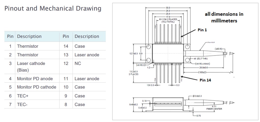
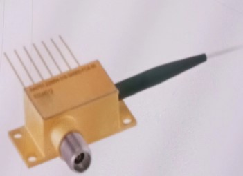
1.1 High Power DFB Lasers, STG-AA1418
40mW in 14-pin butterfly package
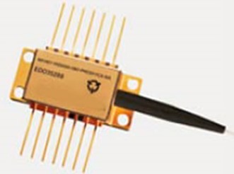
The STG-AA1416 is a CW InGaAs/InP multi-quantum well (MQW) laser diode. The module is ideal in applications where low relative intensity noise (RIN) and stable polarization maintaining properties are needed. The module contains a high efficiency cooler, high performance isolator, thermistor, and monitor detector and is designed and built using our high reliability platform for defense applications.
Key Characteristics:
C-band (1537-1565 nm) wavelengths
40mW ex-fiber output power
Features:
ITU grid wavelengths, 50 or 100GHz spacing
Low RIN
High isolation
High efficiency TEC
Polarization-maintaining or single-mode fiber
Laser welded, hermetically sealed
Built in thermistor and monitor photodiode
Tested to Telcordia GR-468 Core/MIL-STD-883
Applications:
Long haul WDM transmission
RF links
Seeding
Pulsing
Sensing
CATV
Specification:
| Name | Value |
| Wavelength | 1537–1565 nm |
| Output power | Pₒₚ=40mW |
| Laser drive current | Iₒₚ¹: 240–350 mA |
| Linewidth | 2–5 MHz |
| Side mode suppression | 35 dB (P=Pₒₚ) |
| Relative intensity noise | Peak value: -140 dBc/Hz (P=Pₒₚ) |
| Optical isolation | 55 dB (Fₒₚₜ within C-band) |
| Polarization extinction ratio | Min: 20 dB |
| Temperature tuning coefficient | -11 GHz/° C (chip temperature) |
| Kink screening | No kinks, Min: Iₜₕ + 50 mA, Max: 1.1 * Iₒₚ mA |
| Threshold current | Max: 30 mA (Iₜₕ) |
| Operating chip temperature | -20–65° C |
| Laser forward voltage | Max: 3 V (I=Iₒₚ) |
| Monitor photo diode current | Min: 100 µA (P=Pₒₚ) |
| Monitor photo diode dark current | Max: 100nA (Vbias=-5 V) |
| TEC current | 0.1 A (T=25°C), Max: 2.2 A (T=65°C) |
| TEC voltage | 0.1 V (P=Pₒₚ, Tchip = 25° C), Max: 6 V, |
| Thermistor resistance | 9500–10500 Ω (T=25° C) |
| Thermistor β coefficient | 3892 (0 / 50°C) |
| Thermistor Steinhart-Hart coefficients | A = 1.1291e⁻³, B = 2.3413e⁻⁴, C = 8.7674e⁻⁸ |
| Fiber type | PM or non-PM single mode fiber, acrylate |
| Fiber jacket material | Acrylate |
| Fiber core diameter | 8μm |
| Fiber outer diameter | 125μm |
| Fiber buffer diameter | 250μm |
| Fiber length | Min: 1.0 m |
| Fiber bend radius | Min: 35 mm |
| Fiber proof strength | 100kPSI |
| Connector | FC/APC (other connectors available upon request) |
| Output polarization | Polarization parallel to slow axis |
Remark:
1. Iₒₚ and Tₒₚ are defined on device specific test sheet supplied with each unit.
Data Tables
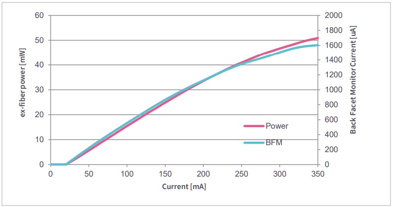
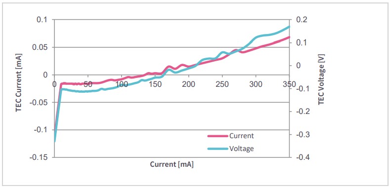
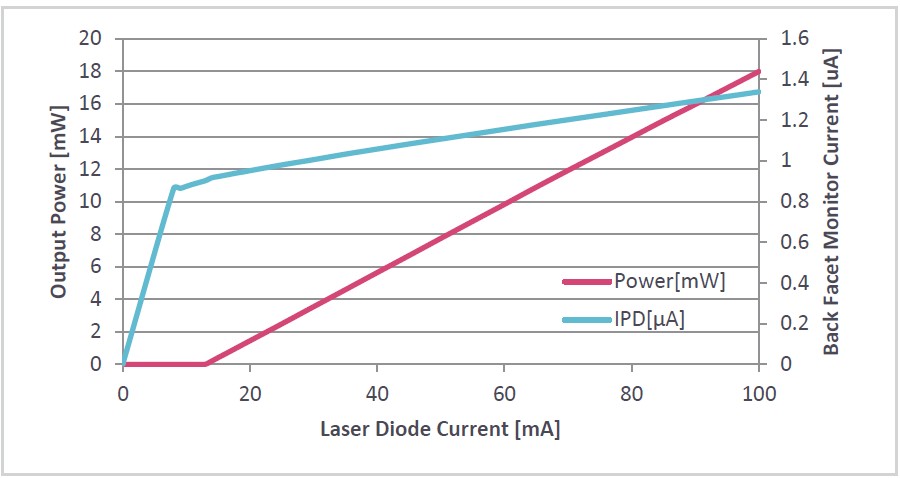
Typical output power and back facet monitor current vs input current
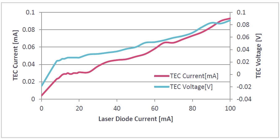
Typical TEC performance Tc=25°C
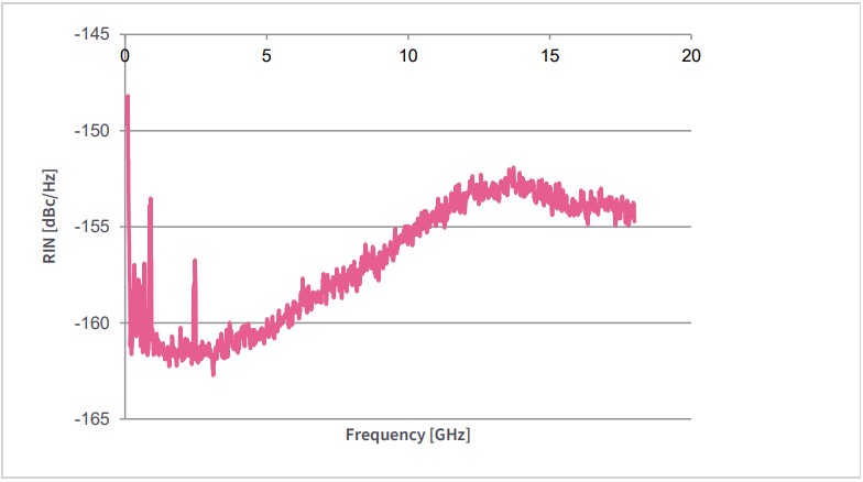
Typical RIN (Relative Intensity Noise) By design, not tested per part
Absolute Maximum Ratings
| Absolute maximum ratings * | Min | Max |
| Storage temperature | -40° C | 85° C |
| Operating case temperature | -20° C | +65° C |
| Laser forward current | 500 mA | |
| Laser reverse voltage | 2 V | |
| Photo diode photo current | 10 mA | |
| Photo diode reverse voltage | 20 V | |
| TEC current | 2.2 A | |
| TEC voltage | 6 V | |
| Thermistor current | 2 mA | |
| Thermistor voltage | 5 V | |
| Lead soldering time | 10 s | |
| Lead soldering temperature | 250° C | |
| ESD (human body model) | 500 V |
* Stresses beyond those listed under “Absolute Maximum Ratings” may cause permanent damage to the device. These are stress ratings only and operation of the device at or beyond these conditions is not implied. Exposure to absolute maximum ratings for extended periods of time may affect device reliability.
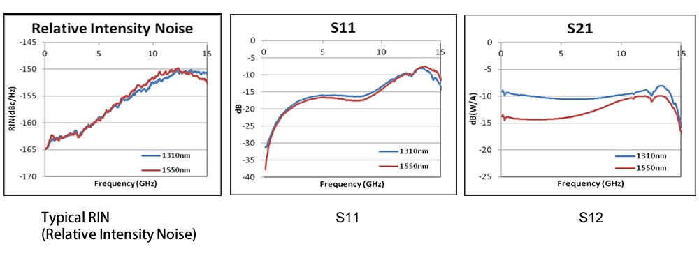
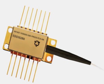
1.2. High Bandwidth DFB Lasers, STG-AA0701
7 PIN K Packaging
The STF-AA0701 distributed feedback laser (DFB) is an InGaAsP/InP multi-quantum well laser diode. This module is ideal for applications where high bandwidth, mode stability, low relative intensity noise (RIN), and stable output power are needed. The STG-AA0701 series contains a thermoelectric cooler, thermistor, back facet monitor detector, and bias tee. The module is designed and built using our high-reliability platform for defence components.
Key Characteristics:
C-band (1537-1565 nm) and 1310nm wavelengths
10 or 18mW ex-fiber output power options
Features:
10 or 18mW output power
High bandwidth
Built in isolator
Ultrafast pulsing capability
Laser welded, hermetically sealed
Built in TEC, thermistor, and monitor detector
Rugged to shock and vibration
Application:
Analog RF links
High speed pulsing
Specification:
| Name | Value |
| Wavelength | 1310±10nm, 1537–1565±1 nm |
| Output power | 18mW (1310 nm), 10mW (1537–1565 nm) |
| Linewidth | Source dependent: Typ: 1 MHz |
| Relative intensity noise | P = Pₒₚ, 0.2-3.0 GHz: Typ: -150 dBc/Hz |
| Side mode suppression | P=Pₒₚ: Min: 30 dB |
| Optical isolation | Fₒₚₜ within C-band, Min: 30 dB, Max: 35 dB ¹ |
| Polarization extinction ratio | Min: 17 dB, Typ: 19 dB |
| Tracking error | P = Pₒₚ, Min: -0.5 dB, Max: 0.5 dB |
| Threshold current | Min: 8 mA, Max: 20 mA |
| Laser drive current | Typ: 75 mA, Max: 100 mA |
| Operating chip temperature | Min: 15 °C, Max: 35 °C |
| Monitor photo diode current | Min: 50 µA |
| Monitor photo diode dark current | 100nA |
| Modulation bandwidth | 3dB from low frequency avg: Min: 10 GHz |
| Electrical back reflection | Max: -10 dB |
| Modulation input matching | 50 Ω |
| TEC current | T amb = 25°C: Typ: 0.1 A, T amb = 70°C: Max: 2.0 A |
| TEC voltage | P=Pₒₚ, T CHIP = 25°C: Typ: 0.1 V, P=Pₒₚ, T CHIP = 25°C: Max: 2.5 V |
| Thermistor resistance | T = 25°C, Min: 9500 Ω, Typ: 9500 Ω, Max: 9500 Ω |
| Thermistor β coefficient | 0 / 50°C: 3892 |
| Thermistor Steinhart-Hart coefficients | A = 1.1291e⁻³, B = 2.3413e⁻⁴, C = 8.7674e⁻⁸ |
| Fiber type | Single-mode, PM or non-PM |
| Fiber core diameter | 8μm |
| Fiber outer diameter | 125μm |
| Fiber buffer diameter | 250μm ² |
| Fiber buffer material | Acrylate ² |
| Fiber length | Min: 1 m |
| Fiber bend radius | 35 mm |
| Output polarization | Parallel to slow axis |
| Connector | FC / APC ³ |
Remark:
1. Reference model number STG-AA0702 for units without internal isolator. SMSR not specified for this model.
2. Optional 900μm loose-tube PVDF buffer recommended for laboratory use.
3. Other connector options available, contact sales for more information
Data Tables
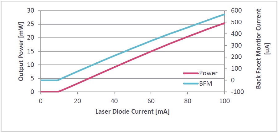
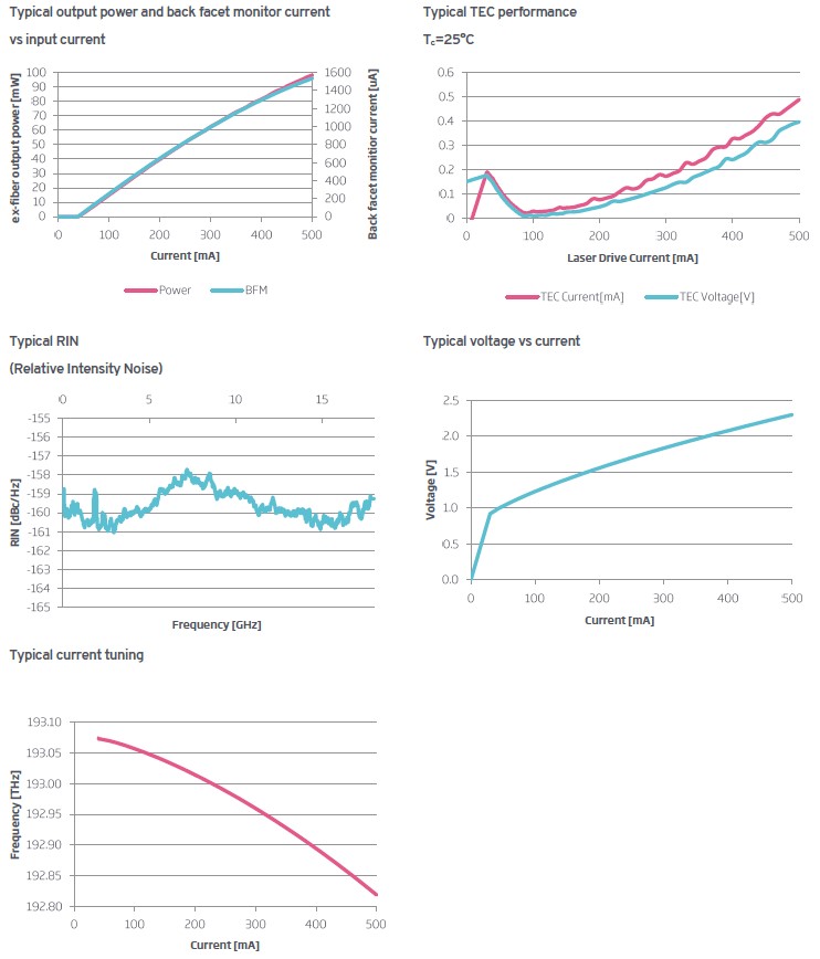
Typical output power and back facet monitor current vs input current (1550 nm)
Typical output power and back facet monitor current vs input current (1310 nm)
Typical TEC performance Tchip=25°C
Absolute Maximum Ratings
| Storage temperature | Min: -40, Max: +85° C |
| Operating case temperature | Min: -20, Max: +70° C |
| Laser forward current | 120 mA |
| Laser reverse voltage | 2 V |
| Photo diode photo current | 10 mA |
| Photo diode reverse voltage | 20 V |
| TEC current | 3 A |
| TEC voltage | 4 V |
| Thermistor current | 2 mA |
| Thermistor voltage | 5 V |
| Lead soldering time | 10 S |
| Lead soldering temperature | 250° C |
| RF input power | 20 dBm |
*Stresses beyond those listed under “Absolute Maximum Ratings” may cause permanent damage to the device. These are stress ratings only and operation of the device at or beyond these conditions is not implied. Exposure to absolute maximum ratings for extended periods of time may affect device reliability.
1.3 High Power DFB Lasers, STG-AA1401
Single frequency lasers in 14-pin butterfly package
Our high power distributed feedback laser (DFB) is an InGaAs/InP multi-quantum well (MQW) laser diode. The module is ideal in applications where low relative intensity noise (RIN) and stable polarization-maintaining properties are needed. The module contains a thermo-electric cooler, thermistor, and monitor detector and is designed and built using our high reliability platform for defence applications.
STG-AA1401 series including STG-AA1402, STG-AA1406, STG-AA1408, and STG-AA1415.
Key Characteristics:
C-band and L-band wavelengths 1537-1565 and 1565-1617 nm
40-100mW ex-fiber output power options
Features:
ITU grid wavelengths, 50 or 100 GHz spacing
Low RIN
PM or SM fiber
High isolation option
Laser welded, hermetically sealed
Built in thermistor and monitor photodiode
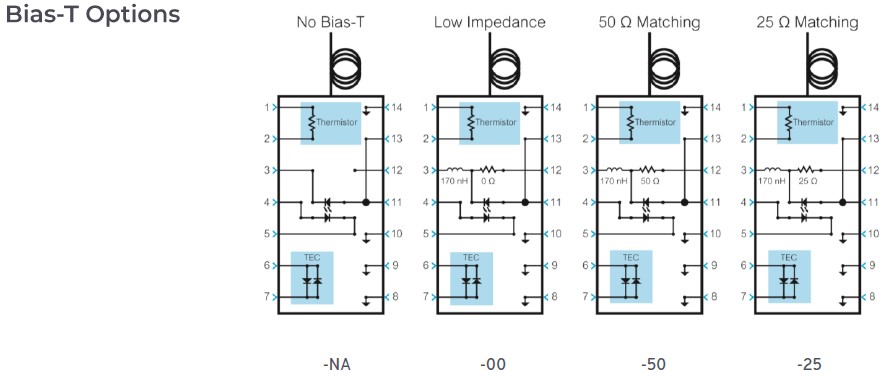
Optional Bias-T
Tested to Telcordia GR-468 Core/MIL-Std 883
Application:
Long haul WDM transmission
RF links
Seeding
Pulsing
Sensing
CATV
Specification:
| Name | Value |
| Wavelength | 1509–1617 nm |
| Output power | 40mW, 50mW, 63mW, 80mW, 100mW |
| Linewidth | Source dependent: 1 MHz |
| Side mode suppression | P=Pₒₚ: 30 dB ¹ |
| Relative intensity noise | P=Pₒₚ, peak value: -150 dBc/Hz |
| Optical isolation | Fₒₚₜ within C-band: Min: 30dB. Max: 35 dB, STG-AA1415-series: Min: 50dB. Max: 55 dB ¹ |
| Polarization extinction ratio | Min: 17 dB, Typ: 21 dB |
| Temperature tuning coefficient | Chip temperature: -12.5 GHz/° C |
| Current tuning coefficient | For reference only, Min: 400 MHz/mA, Max: 800 MHz/mA |
| Relaxation oscillation frequency | For reference only: 6 GHz |
| Kink screening | No kinks, Min: 0.9* Iₒₚ, Max: 1.1* Iₒₚ |
| Threshold current | Typ: 50 mA |
| Laser drive current | 40-63mW models: Typ: 300 mA. Max: 350 mA, 80-100mW models: Typ: 375. Max: 500 mA ² |
| Operating chip temperature | Min: 20 ° C, Max: 40 ° C |
| Laser forward voltage | I=Iₒₚ, Max: 3 V |
| Monitor photo diode current | P=Pₒₚ: 100 µA |
| TEC current | T amb =25°C: Typ: 0.1A, T amb =70°C: Max: 4.0 A |
| TEC voltage | P=Pₒₚ, T CHIP = 25° C, Typ: 0.1 V, Max: 4.0 V |
| Thermistor resistance | T = 25° C, Min: 9500 Ω, Typ: 10000 Ω, Max: 10500 Ω |
| Thermistor β coefficient | 0 / 50°C: 3892 |
| Thermistor Steinhart-Hart coefficients | A = 1.1291e⁻³, B = 2.3413e⁻⁴, C = 8.7674e⁻⁸ |
| Fiber type | PM or non-PM single mode fiber |
| Fiber jacket material | Acrylate ³ |
| Fiber core diameter | 8μm |
| Fiber outer diameter | 125μm |
| Fiber buffer diameter | 250μm ³ |
| Fiber length | Min: 1.0 m |
| Fiber bend radius | Min: 35 mm |
| Fiber proof strength | 100kPSI |
| Connector | FC/APC |
| Output polarization | Polarization parallel to slow axis |
Remark:
1. Reference model number STG-AA1401 for units without internal isolator. SMSR not specified for this model.
2. Iₒₚ and Tₒ ₚp to achieve rated power and frequency at factory test defined on device specific test sheet supplied with each unit.
3. Optional additional 900μm loose-tube PVDF buffer recommended for laboratory use.
4. Other connector options available, contact sales for more information.
Data table (80mW laser shown)
Absolute Maximum Ratings
| Min | Max | |
| Storage temperature | -40° C | 85° C |
| Operating case temperature | -20° C | +70° C |
| Laser forward current, 40-63mW models | 350 mA | |
| Laser forward current, 80-100mW models | 500 mA | |
| Laser reverse voltage | 2 V | |
| Photo diode photo current | 10 mA | |
| Photo diode reverse voltage | 20 V | |
| TEC current | 4A | |
| TEC voltage | 4V | |
| Thermistor current | 2mA | |
| Thermistor voltage | 5V | |
| Lead soldering time | 10s | |
| Lead soldering temperature | 250° C | |
| ESD (human body model) | 500 V |
Remark:
* Stresses beyond those listed under “Absolute Maximum Ratings” may cause permanent damage to the device. These are stress ratings only and operation of the device at or beyond these conditions is not implied. Exposure to absolute maximum ratings for extended periods of time may affect device reliability.
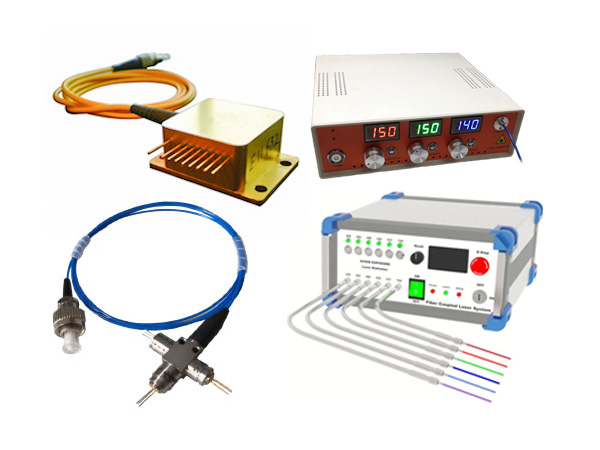
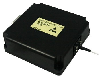
2.1 DFB laser Module, STG-EM650
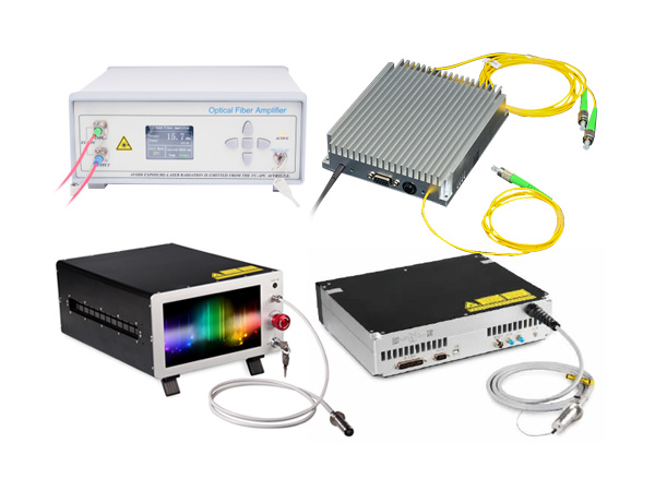
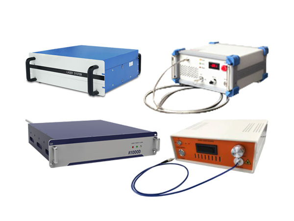
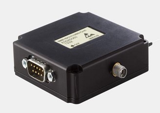
The STG-EM650 integrates a high-power fiber-coupled DFB laser with both an ultra-low noise laser current source and temperature controller. It represents a precision OEM solution for fiber-coupled high power DFB lasers operating with excellent frequency stability, narrow linewidth, low noise, and stable polarization. The module contains a high-power DFB laser, optical isolator, single-mode fiber pigtail, thermo-electric cooler, thermistor, and monitor detector integrated with a laser current source, temperature controller, and monitor detector readout amplifier. The entire module operates from a single +5 V supply. The unit provides a bi-directional power adjust input that may be used for SBS prevention, for constant power operation in conjunction with the monitor detector readout signal and an external control loop, or for finely adjusting the laser oscillation frequency via chirp. The unit also incorporates a bi-directional temperature adjust input for coarse tuning of the laser oscillation frequency. The module is designed and built using our high reliability platform for defence components and incorporates an advanced ultra-low noise laser current source. It drives the internal TEC with a class AB linear H-bridge and incorporates multiple layers of EMI protection. It is our highest performance integrated laser solution and offers performance comparable to laboratory equipment in a much small package.
Key Features:
Integrated current source
Integrated temperature controller
Integrated monitor detector amplifier
High optical output power
ITU wavelengths – Full C band coverage
Low RIN
Narrow linewidth
PM/SM fiber with or without furcation tubing
Key Benefits:
Simple interface
Small form factor
Operates from single +5V supply
Application:
Long haul WDM transmission
RF Links
CATV
Seeding
Sensing
Low-noise high-power source
Specification:
| Name | Value |
| Wavelength | 1310 nm, 1529–1610 nm |
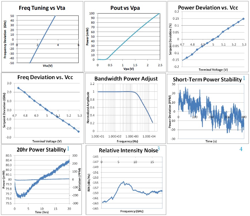
| Optical output power setpoint | Min: Pₒₚ |
| Optical output power fluctuation | 1σ, tₘ = 400s, 0.1s avg&period, Typ: 20 PPM, Max: 50 PPM |
| Long-Term Power Fluctuation | 1σ, tₘ = 20hr, 0.1s avg, 18s period, Typ: 200 PPM, Max: 500 PPM |
| Temperature dependent power drift | -10° ≤ Tₒₚ ≤ 60°: 500 PPM/°C |
| Optical frequency accuracy | Min: -5 GHz, Max: +5 GHz |
| Optical frequency stability | <20 MHz (see note 3) |
| Temperature dependent frequency drift | -10° ≤ Tₒₚ ≤ 60°: Max: ±200 MHz/° C |
| Side mode suppression ratio | Min: 30 dB |
| Polarization extinction ratio | w/ PM fiber only, Min: 17 dB, Typ: 20 dB |
| Optical isolation | Min: 30 dB, Typ: 35 dB |
| Linewidth | 170 kHz |
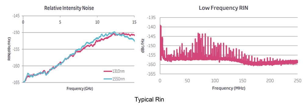
| Relative intensity noise | 50 MHz to 18GHz, Typ: -155 dBc/Hz, Max: -150 dBc/Hz |
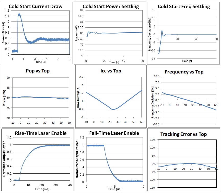
| Cold start settling time | V CC =Vₑₙ 0-5V: 30 s |
| Rise time | (Hot start) Vₑₙ =0-5V: 30 ms |
| Fall time | (Hot Standby) Vₑₙ =5-0V: 5 µs |
| Back facet tracking over temp | Min: -10%, Max: +10% |
| Supply voltage | Typ: 5 V across inputs |
| Supply current | Max: 3 A |
| Laser enable high | Min: 3.5 V |
| Laser enable low | Max: 1.5 V |
| Laser enable input impedance | Typ: 5 kΩ |
| Power adjust | Max: 2.2 V (Warning: see notes) |
| Power adjust input impedance | to 2V Vref: Typ: 1 kΩ |
| Power adjust bandwidth | -3dB: Typ: 8 kHz |
| Temperature adjust | Min: 1.5 V, Max: 3.5 V (Warning: see notes) |
| Temp adjust input impedance | to 2.5V Vref: Typ: 1 kΩ |
| Monitor detector output | at Pₒₚ, Min: 1 V, Max: 3 V |
| Storage temperature | Non-condensing, Min: -40° C, Max: +85° C |
| Operational temperature | temp. at base of module, non-condensing, Min: -10° C, Max: +60° C |
| Fiber type | Single-mode PM or non-PM |
| Fiber core diameter | 8 µm |
| Fiber outer diameter | 125 µm |
| Fiber buffer diameter | 250 µm (optional 900μm loose buffer avail.) |
| Fiber buffer material | Acrylate (optional loose-buffer is PVDF) |
| Fiber length | Min: 1 m |
| Fiber bend radius | Min: 35 mm |
| Connector | FC or SC/APC, key parallel to slow axis; key type is tight-fit/narrow |
| Output Polarization | Parallel to slow axis |
Absolute Maximum Ratings
Stresses beyond those listed may cause permanent damage to the device. These are stress ratings only and operation of the device at these or conditions beyond these is not implied. Exposure to absolute maximum ratings for extended periods of time may affect device reliability.
| Parameter | Condition | Min | Max |
| Storage Temperature | non‐condensing atmosphere | ‐40° C | +85° C |
| Operating Temperature | temp. at base of module, non‐condensing atmosphere | ‐15° C | 65° C |
| Voltage Supply | 4.7 V | 5.5 V | |
| Current Supply | 3.5 A | ||
| Laser Enable Input Voltage | GND‐0.3 V | V CC +0.3 V | |
| Laser Enable Input Current | 2 mA | ||
| Power Adjust Input Voltage | Warning: see notes | 0 V | 2.6 V |
| Power Adjust Input Current Source or Sink | Warning: see notes | ‐3.5 mA | 3.5 mA |
| Temperature Adjust Input Voltage | Warning: see notes | 0 V | 5 V |
| Temperature Adjust Input Current Source or Sink | Warning: see notes | ‐3.5 mA | 3.5 mA |
| Monitor Detector Output Voltage | V CC | V | |
| Monitor Detector Output Current Source or Sink | -15 mA | 15 mA | |
| Optical Output Power | 110mW |
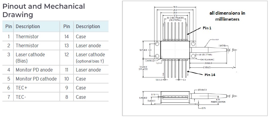
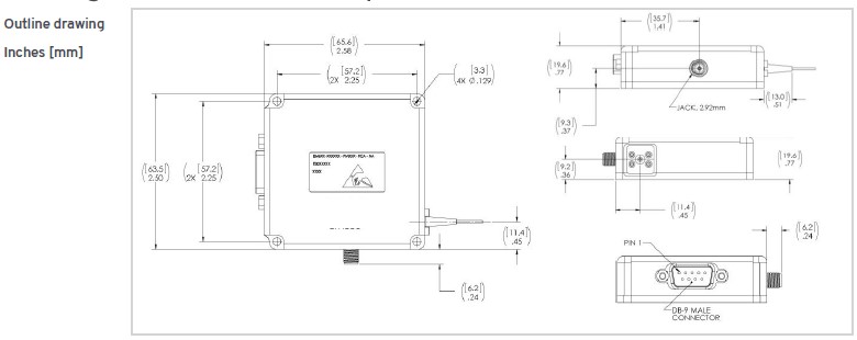
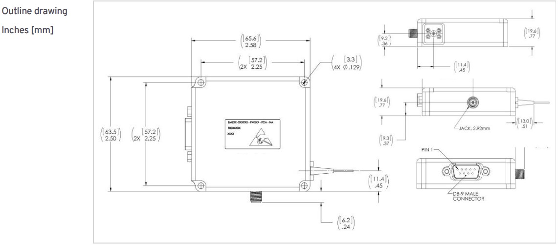
Mechanical drawing
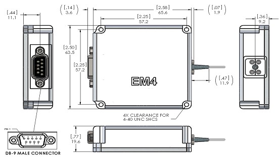
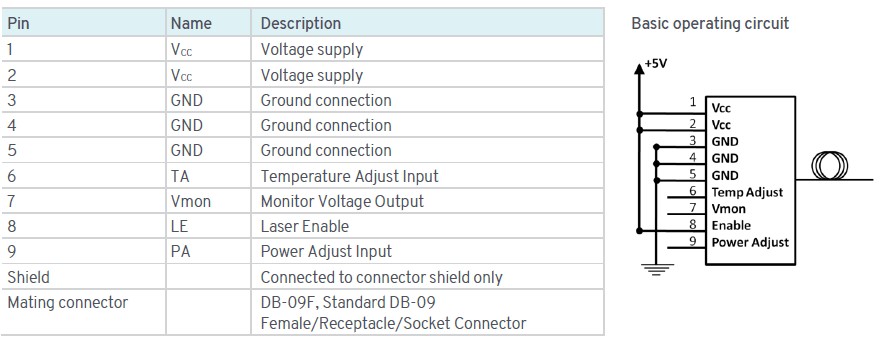
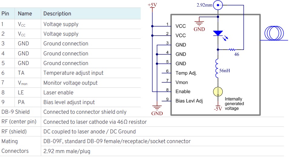
Electrical Connection
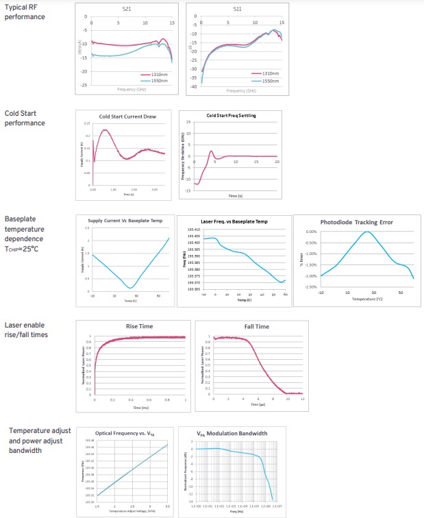
Typical Operating Characteristics (80mW Module)
Typical Operating Characteristics (Continued)
Remark:
1.Power stability of this magnitude is strongly influenced by any movement of the fiber. To duplicate this stability measurement the fiber must be secured and motionless.
2. For 228.849 THz (1310 nm) lasers the laser frequency tolerance is ±1.750 THz (±10 nm).
3. Frequency stability measured by heterodyne of two free running STG-EM650 units over 100s.
4. The peak of the RIN curve corresponds to the relaxation oscillation frequency of the laser which varies in proportion to the drive current above threshold by frelax α ((Ild/Ithreshold) - 1)1/2. Customers employing this device in RIN sensitive applications should therefore be aware that reducing power using the PA input will reduce performance.
NOTES
WARNINGS: several of the parameters listed in the specifications above are denoted with a warning. These warnings are covered by the following notes, which should be understood before operating the device.
Mounting
The STG-EM650 is conductively cooled through its base and needs to be mounted using a thermal interface material to a customer supplied heatsink. We recommend Panasonic PGS series pyrolitic graphite sheets, available in the US from Digi‐Key Corporation. Care should be taken to keep the base temperature of the module between -10 and 60°C at all times during operation.
Noise suppression
The STG-EM650 is a no‐compromises low‐noise integrated laser solution; the temperature controller output is class AB linear, there are no DC/DC converters in the module, the lowest noise components and architectures available are used along with heavy filtering and EMI shielding. Nevertheless, power supply ripple and noise should be minimized and the cable shield should be connected to the STG-EM650 connector shield and tied to the appropriate signal at the power supply end of the cable.
Power Adjust (PA)
The STG-EM650 is designed to run in constant current mode with the drive current set for the as‐ordered output power to achieve the highest possible performance. However, some applications require fine tuning of the laser bias current. The PA input provides this functionality, but its use carries an amount of risk. If bias adjustment is not required this input should be left open. Use of this input carries the potential to overdrive the laser and/or circuitry with the ability to destroy or drastically reduce the device lifetime. No internal protections on this input are provided, but the user is encouraged to clamp or otherwise limit the voltage and current that may be applied to this input.
The default operating power corresponds to an input of 2.05V. For maximum reliability it is recommended that power only be reduced, although if required it can be driven as high as 2.2V (corresponding to a 10% boost in output power). The safest method of using this input is to pull the voltage down using an external resistor or potentiometer to ground. Applying a resistance to ground will create a voltage divide circuit between the external resistance and an internal resistance of 1K to the 2.05V reference. Damage due to overdrive will not be covered under warranty. Use of this input will likely decrease the performance of the STG-EM650 by bypassing its internal ultra‐low noise voltage reference. The PA input must never be shorted directly to Vcc, which would cause circuit malfunction or rapidly destroy the DFB laser.
Temperature Adjust (TA)
The STG-EM650 is designed to operate the laser chip at a constant temperature holding the output frequency within 5 GHz of the ordered frequency. However, some applications require coarse tuning of the output frequency via temperature. In these cases, the laser may be tuned using the TA input. Temperature deviations of more than a few degrees (50 GHz in laser frequency) from the as‐ordered setpoint may result in decreased stability and increases the likelihood of the laser experiencing a longitudinal mode‐hop. The achievable tuning range will depend on the specific laser chip, the ambient temperature, and the thermal resistance to the ambient.Use of this input carries the inherent potential of overdriving the TEC. The TA input is clamped to Vcc through integrated protection diodes. If Vta is established before Vcc these clamp diodes will conduct. The input current should always be limited to ≤3.5mA to prevent destruction of the clamp diodes.
The safest method of driving this input is with a tri-state output whose output is current limited when active, maintained at high‐impedance until Vcc is established, and whose output returns to high‐impedance before Vcc is removed. The device warranty will not be honored for lasers with overdriven TECs. Use of this input also carries the likelihood of decreased frequency stability as it bypasses the internal ultra‐low noise voltage reference.The TA input must never be shorted directly to Vcc or ground which would cause circuit malfunction or rapidly destroy the DFB laser.
Grounding
Care must be taken with grounding, cabling, and connections due to the amount of current the module consumes. Make sure that the voltage on pins PA/TA reference ground as close to the STG-EM650 as possible if either input is connected.
DO NOT connect the cable shield to ground at both ends of the cable to avoid producing a ground loop. #
DO NOT connect the STG-EM650 housing to ground to avoid producing a ground loop.
Startup Considerations
The STG-EM650 consumes a considerable amount of current in the startup phase and when operating at temperature extremes. A voltage source plus cabling able to deliver the maximum specified current at no less than the minimum voltage is therefore needed. Current limiting below the specified maximum during the startup phase will result in an internally measured drive voltage lower than specified. This condition can result in permanent, non‐warrantable damage to the device. If the user fails to sequence the supplies as described in the Power and Temperature adjust sections of this document and Applications Note, the device will immediately suffer non‐warrantable damage or destruction.
Applications Information
Be sure to check this website for the latest applications information for this device. Application note covers general usage of the STG-EM650 along with information particular to tuning via temperature or chirp. If you plan to tune this device, it is highly recommended that you read this app note.
For Application Note, please contact us for more information.
2.2 CWDM Integrated RF Transmitter, STG-EM655
High Bandwidth Directly Modulated DFB laser Module
The STG-EM655 high bandwidth integrated module is a member of our line of high performance single-frequency modules based on precision DFB laser technology. STG-EM655 RF Transmitter integrates a highbandwidth fiber-coupled DFB laser with both an ultra-low noise laser current source and temperature controller. The module also contains an optical isolator and back facet monitor detector readout amplifier. The entire module operates from a single +5 V supply and offers a bi-directional bias adjust input that may be used to control the laser output power or finely adjust the laser oscillation frequency via chirp. The unit also incorporates a bi-directional temperature adjust input for coarse tuning of the laser oscillation frequency. The module is designed and built using our highreliabilityplatform for defense components and incorporates an advanced ultra-low noise laser current source.The STG-EM655 drives the internal TEC with a class AB linear H-bridge and incorporates multiple layers of EMI protection. The device accepts a standard female DB9 connector for the application of power and low-frequency tuning signals while the RF input accepts a standard male 2.92 mm “K” connector. The output optical fiber is available with or without PVDF furcation tubing terminated with a variety of standard opticalconnectors.
Models Available:
1310 nm with 18mW output power
C-band wavelength with 10mW output power
Features:
Integrated current source
Integrated temperature controller
Integrated monitor detector amplifier
SM or PM fiber with or without furcation tubing
Simple interface
Small form factor
Operates from single +5V supply
Application:
RF links
CATV
Seeding
Sensing
Specification:
| Name | Value |
| Optical output power setpoint | 1310 nm devices: Min: 18mW, C-band devices: Min: 10mW |
| Center wavelength | 1310 nm devices, 25°C: Min: λₒₚ -10 nm. Typ: λₒₚ nm. Max: λₒₚ +10 nm, C-band devices, 25°C: Min: λₒₚ -1 nm. Typ: λₒₚ nm. Max: λₒₚ +1 nm |
| Optical output power fluctuation | 1σ, tₘ = 400s, 0.1 s avg and period, Typ: 65 PPM, Max: 100 PPM ¹ |
| Long-Term Power Fluctuation | 1σ, tₘ = 20 hr, 0.1s avg, 18 s period, Typ: 0.1 %, Max: 0.2 % |
| Temperature dependent power drift | -10° C ≤ Tₒₚ ≤ 60° C: ±750 MHz / ° C |
| Side mode suppression ratio | 30 dB |
| Polarization extinction ratio | with PM fiber only, Min: 17 dB, Typ: 20 dB |
| Optical isolation | Min: 30 dB, Typ: 35 dB ² |
| Relative intensity noise | Pₒₚ, 0.2-3 GHz: Typ: -150 dBc/Hz |
| Linewidth | Typ: 1 MHz |
| Cold start settling time | V CC = Vₑₙ 0→5 V: Max: 30 s |
| Rise time | (hot start) Vₑₙ = 0→5 V: Typ: 30 ms |
| Fall time | (hot standby) Vₑₙ =5→0 V: 5 µs |
| Back facet tracking over temp | Min: -10%, Max: +10 |
| Modulation bandwidth | Min: 10 GHz, Typ: 12 GHz |
| Voltage supply | Typ: 5 V across inputs |
| Supply current | Max: 3 A |
| Laser enable high | Min: 3.5 V |
| Laser enable low | Max: 1.5 V |
| Laser enable input impedance | Typ: 5 kΩ |
| Bias level adjust | Warning: see app notes, Min: 0 V, Max: 2.2 V |
| Bias level adjust input impedance | to 2V VREF: Typ: 1 kΩ |
| Bias level adjust bandwidth | -3dB: Typ: 8 kHz |
| Temperature adjust | Warning: see app notes, Min: 1.5 V, Max: 3.5 V |
| Temp adjust input impedance | to 2.5 V VREF: Typ: 1 kΩ |
| Monitor detector output | at Pₒₚ, Min: 1 V, Max: 3 V |
| Bias tee inductance | 53nH |
| Fiber type | Single-mode, PM or non-PM |
| Fiber core diameter | 8μm |
| Fiber outer diameter | 125μm |
| Fiber buffer diameter | 250μm ⁴ |
| Fiber buffer material | Acrylate ⁴ |
| Fiber length | Min: 1 m |
| Fiber bend radius | Min: 35 mm |
| Output Polarization | Parallel to slow axis |
| Connector | FC/APC ⁵ |
Remark:
1.Power stability of this magnitude is strongly influenced by any movement of the fiber. To duplicate this stability measurement the fiber must be secured and motionless.
2.Units are available without isolator (product series STG-EM656). Devices without optical isolators are subject to mode-hops and are susceptible to back reflections. The wavelength stability devices with no optical isolator cannot be guaranteed.
3. The peak of the RIN curve corresponds to the relaxation oscillation frequency of the laser which varies in proportion to the drive current above threshold by f relax α ((I ld /I threshold ) - 1)1/2. Customers employing this device in RIN sensitive applications should therefore be aware that reducing the bias level using the power adjust input will reduce performance. Reducing the bias level reduces the device modulation bandwidth by the same relationship.
4. Optional 900 μm loose-tube PVDF buffer recommended for laboratory use.
5. Other connector options available, contact sales for more information.
Max Ratings
| Absolute Maximum Ratings* | Min | Max |
| Storage temperature | -40° C | 85° C |
| Operating case temperature (at base of module) | -10° C | +60° C |
| Voltage supply | 4.6V | 5.5V |
| Current supply | 3.5A | |
| Laser enable input voltage | GND-0.3V | VCC + 0.3V |
| Laser enable input current | 2mA | |
| Blas adjust input voltage (warning, see notes) | 0V | 2.4V |
| Bias adjust input current source or sink (warning, see notes) | -3.5mA | 3.5mA |
| Temperature adjust input voltage (warning, see notes) | 0V | 5V |
| Temp. adjust input current source or sink (warning, see notes) | -3.5mA | 3.5mA |
| Monitor detector output voltage | VCCV | |
| Monitor detector output current source or sink | -15mA | 15mA |
| Optical output power | 20mW |
Remark:
* Stresses beyond those listed under “absolute maximum ratings” may cause permanent damage to the device. These are stress ratings only and operation of the device at or beyond these conditions is not implied. Exposure to absolute maximum ratings for extended periods of time may affect device reliability.
Drawing and performance Graphs
Drawings and performance graphs,continued
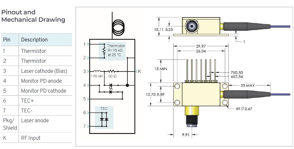
Pinout
Application Notes
Mounting
The STG-EM655 is conductively cooled through its base and needs to be mounted using a thermal interface material to a customer supplied heatsink. We recommend Panasonic PGS series pyrolitic graphite sheets, available in the US from Digi-Key Corporation.
Do not use graphite sheets with adhesive backing.
Care should be taken to keep the base temperature of the module between -10 - 60°C at all times during operation.
Noise Suppression
The STG-EM655 is a no-compromises low noise integrated laser solution; the temperature controller output is class AB linear, there are no DC/DC converters in the module, the lowest noise components and architectures available are used along with heavy filtering and EMI shielding. Nevertheless, power supply ripple and noise should be minimized and the cable shield should be connected to the STG-EM655 connector shield and tied to the appropriate signal at the power supply end of the cable.
Bias Level Adjust (PA)
The STG-EM655 is designed to run in constant current mode with the drive current set for the as-ordered output power to achieve the highest possible performance. However, some applications require fine tuning of the laser bias current. The PA input provides this functionality, but its use carries an amount of risk. If bias adjustment is not required this input should be left open. Use of this input carries the potential to overdrive the laser and/or circuitry with the ability to destroy or drastically reduce the device lifetime. No internal protections on this input are provided, but the user is encouraged to clamp or otherwise limit the voltage and current that may be applied to this input.
The default operating power corresponds to an input of 2.05 V. For maximum reliability it is recommended that power only be reduced, although if required it can be driven as high as 2.2 V (corresponding to a 10% boost in output power). The safest method of using this input is to pull the voltage down using an external resistor or potentiometer to ground.
Applying a resistance to ground will create a voltage divide circuit between the external resistance and an internal resistance of 1 K to the 2.05 V reference. Damage due to overdrive will not be covered under warranty. Use of this input will likely decrease the performance of the STG-EM655 by bypassing its internal ultra-low noise voltage reference.
Warning: The PA input must never be shorted directly to V CC which would cause circuit malfunction or rapidly destroy the laser.
Temperature Adjust (TA)
The STG-EM655 is designed to operate the laser chip at a constant temperature of 25° C holding the output frequency within a window of 5 GHz. However, some applications require coarse tuning of the output frequency via temperature. In these cases, the laser may be tuned using the TA input. Temperature deviations of more than a few degrees (50 GHz in laser frequency) may result in decreased stability and increases the likelihood of the laser experiencing a longitudinal mode-hop. Use of this input carries the inherent potential of overdriving the TEC. The TA input is clamped to V CC through integrated protection diodes.
If V ta is established before V CC these clamp diodes will conduct. The input current should always be limited to ≤3.5 mA to prevent destruction of the clamp diodes. The safest method of driving this input is with a tristate output whose output is current limited when active, maintained at high impedance until V CC is established, and whose output returns to high-impedance before V CC is removed. The device warranty will not be honored for lasers with overdriven TECs. Use of this input also carries the likelihood of decreased frequency stability as it bypasses the internal ultra-low noise voltage reference.
Warning: The TA input must never be shorted directly to V CC or ground which would cause circuit malfunction or rapidly destroy the laser.
Grounding, DC to RF
Care must be taken with grounding, cabling, and connections due to the amount of current the module consumes. Make sure that the voltage on pins PA/TA reference ground as close to the STG-EM655 as possible if either input is connected.
DO NOT connect the cable shield to ground atboth ends of the cable to avoid producing a ground loop.
DO NOT connect the STG-EM655 housing to ground to avoid producing a ground loop.
The shield of the RF input 2.92 mm connector is connected to the laser anode and the centerconductor to the laser cathode via the RF matching resistor. Care should be taken that the connection of an RF source does not result in a DC leakage path. The ground of the RF source must be isolated from the ground of the DC power supply, as 1.3 V typical bias voltage difference will exist between the RF ground and DC ground due to the laser diode bias voltage. In addition, shorting of the RF connector places an electrical short in parallel with the laser which will prevent the laser from operating.
Startup Considerations
The STG-EM655 consumes a considerable amount of current in the startup phase and when operating at temperature extremes. A voltage source plus cabling able to deliver the maximum specified current at no less than the minimum voltage is therefore needed. Current limiting below the specified maximum during the startup phase will result in an internally measured drive voltage lower than specified. This condition can result in permanent, non-warrantable damage to the device.
Warning: If the user fails to sequence the supplies as described in the Power and Temperature Adjust sections of this document and Applications Note, the device will immediately suffer non-warrantable damage or destruction.
Power Supply
This device requires between 4.6 V and 5.5 V as measured from the V CC to ground terminals. These voltages must be maintained for currents ranging from 0-3A necessitating the use of short wires and/or large AWG wire.
Warning: Failure to supply sufficient voltage at the device terminals may result in excess current draw and permanent, non-warrantable damage. If the device draws 3A for more than 10 seconds, turn off power and check for excessive wiring resistance or a baseplate temperature outside the operational range.
Additional Information
Be sure to check this website for the latest application information for this device.
Application note covers general usage of the STG-EM655 along with information particular to tuning via temperature or chirp. If you plan to tune this device, we highly recommended that you read this application note.
For Application Note, please contact us for more information.
2.3 CWDM Integrated RF Transmitter, STG-EM657
High Bandwidth Directly Modulated DFB Laser Module
The STG-EM657 high bandwidth integrated module is a member of our line of high performances single-frequency modules based on precision DFB laser technology. The STG-EM657 RF Transmitter integrates high bandwidth fiber-coupled DFB laser with both an ultra-low noise laser current source and temperature controller. The module also contains an optical isolator and back facet monitor detector readout amplifier. The entire module operates from a single +5 V supply and offers a bi-directional bias adjust input that may be used to control the laser output power or finely adjust the laser oscillation frequency via chirp. The unit also incorporates a bi-directional temperature adjust input for coarse tuning of the laser oscillation frequency. The module is designed and built using our high reliability platform for defence components and incorporates an advanced ultra-low noise laser current source. The STG-EM657 drives the internal TEC with a class AB linear H-bridge and incorporates multiple layers of EMI protection. The device accepts a standard female DB9 connector for the application of power and low-frequency tuning signals while the RF input accepts a standard male 2.92 mm “K” connector. The output optical fiber is available with or without PVDF furcation tubing terminated with a variety of standard optical connectors.
Models Available:
1310 nm and C-band wavelength options with 18mW and 10mW output power respectively
Features:
Integrated current source
Integrated temperature controller
Integrated monitor detector amplifier
SM or PM fiber with or without furcation tubing
Simple interface
Small form factor
Operates from single +5 V supply
Application:
RF links
CATV
Seeding
Sensing
Specification:
| Name | Value |
| Optical output power setpoint | 1310 nm devices: Min: 18mW, C-band devices: Min: 10mW |
| Center wavelength | 1310 nm devices, 25°C: Min: λₒₚ -10 nm. Typ: λₒₚ nm. Max: λₒₚ +10 nm, C-band devices, 25°C: Min: λₒₚ -1 nm. Typ: λₒₚ nm. Max: λₒₚ +1 nm |
| Optical output power fluctuation | 1 σ, tₘ = 400 s, 0.1 s avg and period, Typ: 65 PPM, Max: 100 PPM ¹ |
| Long-Term Power Fluctuation | 1 σ, tₘ = 20 hr, 0.1 s avg, 18 s period, Typ: 0.1%, Max: 0.2% |
| Temperature dependent power drift | -10° C ≤ Tₒₚ ≤ 60° C: Typ: 0.35 % / ° C |
| Temperature dependent frequency drift | -10° C ≤ Tₒₚ ≤ 60° C: Max: ±750 MHz / ° C |
| Side mode suppression ratio | 30 dB |
| Polarization extinction ratio | with PM fiber only, Min: 17 dB, Max: 20 dB |
| Optical isolation | Min: 30 dB, Typ: 35 dB ² |
| Relative intensity noise | Pₒₚ, 0.2-3 GHz@: Typ: -150 dBc / Hz |
| Linewidth | Typ: 4 MHz |
| Cold start settling time | V CC = V EN 0 - 5V: Max: 10 s |
| Rise time | (hot start) V EN = 0 -5V: Typ: 120 µs |
| Fall time | (hot standby) V EN =5 - 0V: Typ: 3.8 µs |
| Back facet tracking over temp | Min: -10 %, Max: +10 % |
| Modulation bandwidth | Min: 10 GHz, Typ: 12 GHz |
| Voltage supply | Typ: 5 V across inputs |
| Current supply | Max: 3.5 A |
| Laser enable high | Typ: 2.9 V |
| Laser enable low | Typ: 2.9 V |
| Laser enable input impedance | Typ: 5 MΩ |
| Bias level adjust | Warning: see app notes, Min: 0 V, Max: 2.2 V ³ |
| Bias level adjust input impedance | to 2V VREF: Typ: 9.74 kΩ |
| Bias level adjust bandwidth | -3dB: Typ: 400 kHz |
| Temperature adjust | Warning: see app notes, Min: 1.55 V, Max: 3.45 V |
| Temp adjust input impedance | to 2.5V VREF: Typ: 1 kΩ |
| Monitor detector output | at Pₒₚ, Min: 1 V, Max: 3 V |
| Bias tee inductance | Typ: 53nH |
| Fiber type | Single-mode, PM or non-PM |
| Fiber core diameter | 8μm |
| Fiber outer diameter | 125μm |
| Fiber buffer diameter | 250μm ⁴ |
| Fiber buffer material | Acrylate ⁴ |
| Fiber length | Min: 1 m |
| Fiber bend radius | Min: 35 mm |
| Output Polarization | Parallel to slow axis |
| Connector | FC/APC ⁵ |
Remark:
1.Power stability of this magnitude is strongly influenced by any movement of the fiber. To duplicate this stability measurement the fiber must be secured and motionless.
2.Units are available without isolator. Devices without optical isolators are subject to mode-hops and are susceptible to back reflections. The wavelength stability devices with no optical isolator cannot be guaranteed.
3.The peak of the RIN curve corresponds to the relaxation oscillation frequency of the laser which varies in proportion to the drive current above threshold by f relax α ((I ld /I threshold ) - 1) 1/2. Customers employing this device in RIN sensitive applications should therefore be aware that reducing the bias level using the power adjust input will reduce performance. Reducing the bias level reduces the device modulation bandwidth by the same relationship.
4. Optional 900 μm loose-tube PVDF buffer recommended for laboratory use.
5. Other connector options available, contact sales for more information.
Max Ratings
| Absolute Maximum Ratings* | Min | Max |
| Storage temperature | -40° C | 85° C |
| Operating case temperature (at base of module) | -10° C | +60° C |
| Voltage supply | 4.6V | 5.5V |
| Current supply | 4A | |
| Laser enable input voltage | GND-0.3V | VCC + 0.3V |
| Laser enable input current | 2mA | |
| Blas adjust input voltage (warning, see notes) | 0V | 2.4V |
| Bias adjust input current source or sink (warning, see notes) | -3.5mA | 3.5mA |
| Temperature adjust input voltage (warning, see notes) | 0V | 5V |
| Temp. adjust input current source or sink (warning, see notes) | -3.5mA | 3.5mA |
| Monitor detector output voltage | VCCV | |
| Monitor detector output current source or sink | -15mA | 15mA |
| Optical output power | 20mW |
Drawing and performance Graphs
Drawings and performance graphs,continued
Pinout
Application Notes
Mounting
The STG-EM657 is conductively cooled through its base and needs to be mounted using a thermal interface material to a customer supplied heatsink. Do not use graphite sheets with adhesive backing as the adhesive is an insulator. Care should be taken to keep the base temperature of the module between -10 - 60°C at all times during operation.
Bias Level Adjust (PA)
The STG-EM657 is designed to run in constant current mode with the drive current set for the as-ordered output power to achieve the highest possible performance. However, some applications require fine tuning of the laser bias current. The PA input provides this functionality, but its use carries an amount of risk. If bias adjustment is not required this input should be left open. Use of this input carries the potential to overdrive the laser with the ability to destroy or drastically reduce the device lifetime. No internal protections on this input are provided, but the user is encouraged to clamp or otherwise limit the voltage and current that may be applied to this input.
The default operating power corresponds to an input of 2.05 V. For maximum reliability it is recommended that power only be reduced, although if required it can be driven as high as 2.2 V (corresponding to a 10% boost in output power). The safest method of using this input is to pull the voltage down using an external resistor or potentiometer to ground. Applying a resistance to ground will create a voltage divide circuit between the external resistance and an internal resistance of 9.74 K to the 2.05 V reference.
Damage due to overdrive will not be covered under warranty. Use of this input will likely decrease the performance of the STG-EM657 by bypassing its internal ultra-low noise voltage reference.
Warning: The PA input must never be shorted directly to V CC which would cause circuit malfunction or rapidly destroy the laser.
Temperature Adjust (TA)
The STG-EM657 is designed to operate the laser chip at a constant temperature of 25°C holding the output frequency within a window of 5 GHz. However, some applications require coarse tuning of the output frequency via temperature. In these cases, the laser may be tuned using the TA input. Temperature deviations of more than a few degrees (50 GHz in laser frequency) may result in decreased stability and increases the likelihood of the laser experiencing a longitudinal mode-hop.
Use of this input carries the inherent potential of overdriving the TEC. The TA input is clamped to V CC through integrated protection diodes. If V ta is established before V CC these clamp diodes will conduct. The input current should always be limited to ≤3.5 mA to prevent destruction of the clamp diodes. The safest method of driving this input is with a tristate output whose output is current limited when active, maintained at high impedance until V CC is established, and whose output returns to high-impedance before V CC is removed.
The device warranty will not be honored for lasers with overdriven TECs. Use of this input also carries the likelihood of decreased frequency stability as it bypasses the internal ultra-low noise voltage.
Warning: The TA input must never be shorted directly to V CC or ground which would cause circuit malfunction or rapidly destroy the laser.
Grounding, DC to RF
Care must be taken with grounding, cabling, and connections due to the amount of current the module consumes. Make sure that the voltage on pins PA/TA reference ground as close to the STG-EM657 as possible if either input is connected.
DO NOT connect the cable shield to ground at both ends of the cable to avoid producing a ground loop.
The shield of the RF input 2.92 mm connector is connected to the laser anode and the center conductor to the laser cathode via the RF matching resistor. RF source should be AC coupled to the RF input. The RF and DC ground are at laser anode potential. An internal switching regulator is used to provide a negative reference to bias the laser.
The presence of this switching regulator allows for more convenient operation in systems where the RF and DC supply must have the same ground, but increases the noise level of the STG-EM657 relative to the STG-EM655 or STG-EM650. The switching regulator noise causes a broadening of the laser line width to approximately 4MHz, and switching harmonics are visible in the low frequency RIN of the laser. This noise is no longer significant at frequencies greater than 200 MHz, and thus should not impact most high speed communication applications.
Startup Considerations
The STG-EM657 consumes a considerable amount of current in the startup phase and when operating at temperature extremes. A voltage source plus cabling able to deliver the maximum specified current at no less than the minimum voltage is therefore needed. Current limiting below the specified maximum during the startup phase will result in an internally measured drive voltage lower than specified. This condition can result in permanent, non-warrantable damage to the device.
Warning: If the user fails to sequence the supplies as described in the Power and Temperature Adjust sections of this document and Applications Note, the device will immediately suffer non-warrantable damage or destruction.
Power Supply
This device requires between 4.6 V and 5.5 V as measured from the V CC to GND terminals. These voltages must be maintained for currents ranging from 0-3.5 A necessitating the use of short wires and/or large AWG wire.
Warning: Failure to supply sufficient voltage at the device terminals may result in excess current draw and permanent, non-warrantable damage. If the device draws 3.5 A for more than 10 seconds, turn off power and check for excessive wiring resistance or a baseplate temperature outside the operational range.
Additional Information
Be sure to check the website for the latest application information for this device. Application note covers general usage of the STG-EM657 along with information particular to tuning via temperature or chirp. If you plan to tune this device, we highly recommended that you read this application note.
For Application Note, please contact us for more information.
We offer DFB/ DBR/ VCSEL laser, which is special designed for gas detection such as CH4, H2S, NH3, H2O, CO, CO2, C2H4, HF, C2H2, etc. Features with narrow linewidth up to 2MHz, ultra compact dimension, high power and wavelength stability, they are widely used in fiber gas detection, seed light source, fiber optical sensing field, etc.
Features:
Stable wavelength and output power;
Narrow linewidth;
No jump mode output in operating current range
Applications:
Optical fiber gas detection system;
Optical sensing;
Fiber communications
| as Composition | Chemical Formula | Absorption Spectrum |
| Methane | CH4 | 1650.9 nm, 1653.7 nm |
| Hydrogen sulfide | H2S | 1578 nm, 1590 nm |
| Ammonia | NH3 | 1512 nm |
| Carbon monoxide | CO | 1567 nm |
| Carbon dioxide | CO2 | 1580 nm |
| Acetylene | C2H2 | 1532.68 nm |
| Ethylene | C2H4 | 1620 nm, 1625 nm, 1627 nm |
| Hydrogen fluoride | HF | 1268.7 nm, 1273 nm, 1305 nm, 1312 nm |
| Water | H2O | 1368 nm, 1392 nm |
| Model | Wavelength | Output Power |
| STC-TEM-F-1268DFB | 1268 nm | 1-10 mW |
| STC-TEM-F-1273DFB | 1273 nm | 1-10 mW |
| STC-TEM-F-1305DFB | 1305 nm | 1-10 mW |
| STC-TEM-F-1310DFB | 1310 nm | 1-10 mW |
| STC-TEM-F-1312DFB | 1312 nm | 1-10 mW |
| STC-TEM-F-1368DFB | 1368 nm | 1-10 mW |
| STC-TEM-F-1392DFB | 1392 nm | 1-10 mW |
| STC-TEM-F-1450DFB | 1450 nm | 1-20 mW |
| STC-TEM-F-1470DFB | 1470 nm | 1-20 mW |
| STC-TEM-F-1490DFB | 1490 nm | 1-20 mW |
| STC-TEM-F-1512DFB | 1512 nm | 1-10 mW |
| STC-TEM-F-1532DFB | 1532 nm | 1-20 mW |
| STC-TEM-F-1540DFB | 1540 nm | 1-20 mW |
| STC-TEM-F-1550DFB | 1550 nm | 1-30 mW |
| STC-TEM-F-1560DFB | 1560 nm | 1-20 mW |
| STC-TEM-F-1567DFB | 1567 nm | 1-10 mW |
| STC-TEM-F-1573DFB | 1573 nm | 1-20 mW |
| STC-TEM-F-1578DFB | 1578 nm | 1~10 mW |
| STC-TEM-F-1580DFB | 1580 nm | 1~10 mW |
| STC-TEM-F-1590DFB | 1590 nm | 1-20 mW |
| STC-TEM-F-1610DFB | 1610 nm | 1-20 mW |
| STC-TEM-F-1620DFB | 1620 nm | 1~10 mW |
| STC-TEM-F-1625DFB | 1625 nm | 1~10 mW |
| STC-TEM-F-1627DFB | 1627 nm | 1~10 mW |
| STC-TEM-F-1651DFB | 1651 nm | 1~10 mW |
| STC-TEM-F-1653DFB | 1653 nm | 1~10 mW |
We offer wavelength tunable laser, the output wavelengths can be changed continuously within a certain range. Tunable lasers come with good beam quality, high stability and long life time, they are widely used in spectroscopy, photochemistry, medicine, biology, integrated optics, laser processing, etc.
Features:
Good beam quality;
Compact design;
High stability;
Long life time;
Easy operation
Applications:
Spectroscopy;
Medicine; Photochemistry;
Biology;
Integrated optics
Tunable Diode Laser
| Tunable Wavelength Band | Model | Output Power | Spectral Linewidth |
| 403~407 nm | STC-TUN-403~407 | 1~30 mW | <0.1 nm |
| 408~412 nm | STC-TUN-408~412 | 1~30 mW | <0.1 nm |
| 448~452 nm | STC-TUN-448~452 | 1~10 mW | <0.1 nm |
| 518~522 nm | STC-TUN-518~522 | 1~10 mW | <0.1 nm |
| 634~643 nm | STC-TUN-634~643 | 1~10 mW | <0.1 nm |
| 652~658 nm | STC-TUN-652~658 | 1~10 mW | <0.1 nm |
Tunable Ti:Sapphire Laser
| Tunable Wavelength Band | Model | Output Power | Spectral Linewidth |
| 770~840 nm | STC-TUN-TiN-770~840 | 1~400 mW | <40 pm |
| 770~840 nm | STC-TUN-Ti-770~840 | 1~1000 mW | <2 nm |
| 770~840 nm | STC-TUN-TiA-770~840 | 1~1300 mW | <2 nm |
Tunable Infrared Laser
| Tunable Wavelength Band | Model | Output Power | Spectral Linewidth |
| 1400~1800 nm | STC-TUN-W-1400~1800 | 1~2000 mW | <2 nm |
| 2600~4450 nm | STC-TUN-W-2600~4450 | 1~1000 mW | <2 nm |
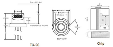
The STDL-DFB 6 XXXX series is an InGaAsP based distributed feedback laser series in available in a TO 56 package, with an aspherical lens 1653 nm wavelength for gas sensing is available in BTF chip form. These devices have been optimized for & photonics telecommunication, test measurements as well as sensing applications. 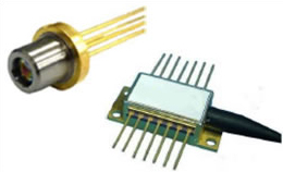
Applications
OTDR
Photonic Sensing (gas)
Biomedical Sensing
Telecommunication
Features & Performance
Uncooled 16xx n m DFB laser
Operating temperature from -5C to 70C
1653nm selection for Gas Sensing
Optical output min. 3mW (TO)
| Part No | nm | Po (mW) | Pkg |
| STDL-DFB65003T-A | 1650 | 3 | TO-56 |
| STDL-DFB62503T-A | 1625 | 3 | TO-56 |
| STDL-DFB61003T-A | 1610 | 3 | TO-56 |
| STDL-DFB65306D | 1653 | 6 | Chip |
| STDL-DFB65304D | 1653 | 4 | Chip |
| STDL-DFB65303T-A | 1653 | 3 | TO |
Customised wavelengths available.
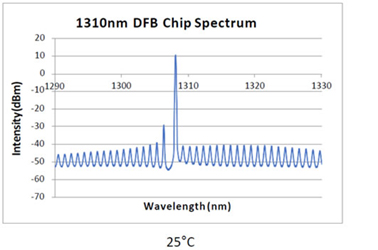
The STDL-DFB31020D is an InGaAsP based distributed feedback laser chips. These devices have been optimized for telecommunication test & measurements as well as Datacom applications.
Applications
OTDR
FTTx
PSM-4
CWDM
Features & Performance
Uncooled operation from 5 to 70°C
Output power (CW) of 20mW at 25°C, Iop 47mA (typical)
Typical SMSR >=35dB
Designed for CW transmission
| Part No. | Wavelength nm | Laser power Po (mW) | Pkg |
| STDL-DFB31020D | 1310 | 20 | Chip |
| STDL-DFB31040D | 1310 | 40 | Chip |
| STDL-DFB31070D | 1310 | 70 | Chip |
Custom wavelengths available.
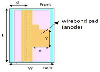
| Parameters | Symbol | Typical | Unit |
| Chip Size | L x W xH | 250* x 200 x100 | mm |
| Emission Spot (from Chip Edge) | d | 65 | mm |
| Wire Bond Pad | x,y | 100 x100 | mm |
*L is longer, for higher power devices.
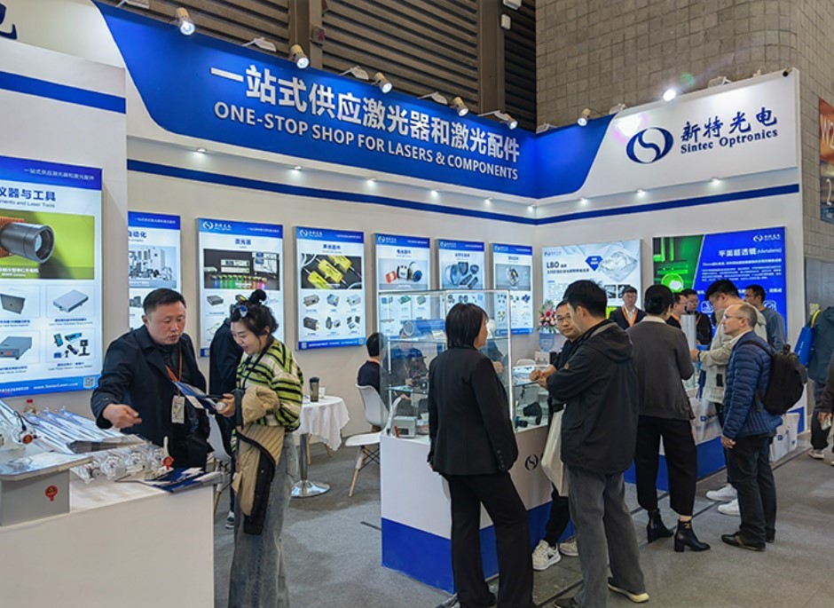
A leading supplier and manufacturer of a wide range of photonics products such as lasers,laser parts & machines.
Office: 10 Bukit Batok Crescent #07-02 The Spire Singapore 658079
Tel: +65 63167112
Fax: +65 63167113
Whatsapp: +65 91904616