 English
 Français
 Deutsch
 euskara
 Русский язык
 Italiano
 Português
 Nederlands
 Polski
 Greek
Greek Lietuva
 Türkçe
 日本語
日本語 한어
한어 中文
中文 தாமில்
 فارسی
فارسی हिंदी
हिंदी Tiếng Việt
 ภาษาไทย
 Pilipino
 Indonesia
 தாமில்
Send us a message
CLOSE


")
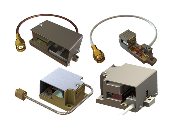
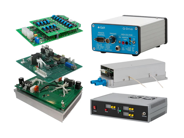
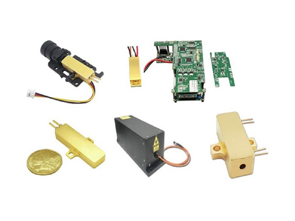
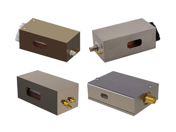
An RF driver generates a fixed or variable frequency signal supplied to the acousto-optic device’s transducer. This in turn uses the piezoelectric effect to very precisely convert the RF signal to an acoustic wave that propagates within the acousto-optic device’s crystal. The frequency and intensity of the applied signal will determine how much an optical beam is modulated, deflected, or tuned.
An acousto-optic device and its RF driver should be selected as a unit to optimize speed and stability for each application. Additional driver features include first pulse suppression, synchronization, pulse shaping, and multichannel operation. We offer a wide variety of stable high frequency drivers with analog and digital modulation capability. Voltage controlled oscillators (VCOs) vary the oscillation frequency via the input voltage, and are a costeffective solution for applications with less stringent frequency stability and linearity requirements.
Direct digital synthesizer (DDS) drivers offer higher stability, with fast switching time and high resolution. They can create random waveforms from a single, fixed-frequency reference clock, and thus are ideal for pulse shaping and special functions. They also allow frequency to be varied on the order of a few hundred nanoseconds, and are inherently very linear. DDS drivers are software driven, and can be run from a user-friendly interface (a GUI), or controlled directly via computer driver commands. Our high-performance multi-frequency DDS drivers generate up to 8 channels of RF frequencies simultaneously.
As our AO product lines expand, we are creating more flexible, adaptive RF drivers with dual analog/digital operation and configurable firmware to accommodate functionality like triggering and temperature control without the need for new hardware. Our OEM designs, in contrast, are optimized to each customer’s application, maximizing performance in the required form factor.
CHOOSING AN RF DRIVER
The needs of the AO device will dictate the choice of RF driver. The primary factors to consider are shown below, though speed, duty cycle, and special functions are also important.
MODULATION: DIGITAL VS ANALOG
The modulation mode determines how the applied RF power is varied, and thus the intensity of diffracted light. In digital modulation, the RF power is applied in an on/off state via an applied TTL signal, thus controlling whether the beam is diffracted. In analog modulation, the RF power is controlled through application of a voltage within a specified range, yielding control over the diffraction efficiency and allowing shaping of that waveform in time.
FIXED VS VARIABLE FREQUENCY DRIVERS
Fixed frequency drivers provide a single output frequency which is matched to the AO device. Offered from 24-440 MHz, fixed frequency drivers may be controlled via analog or TTL input, some with manually adjustable output RF power. These are used most often for modulation applications.
Variable and programmable frequency RF drivers allow active control of output frequency. Voltage controlled oscillators (VCOs) provide a linearly swept (variable) RF drive frequency, and are flexible enough to be used for any AO device. Direct digital synthesizer (DDS) drivers offer programmable frequency. They can create random waveforms from a single, fixed-frequency reference clock, and thus are ideal for pulse shaping and special functions. DDS drivers are software driven, and can be run from a user-friendly interface (a GUI), or controlled directly via computer driver commands. Our high-performance multi-frequency DDS drivers generate up to 8 channels of RF frequencies simultaneously.
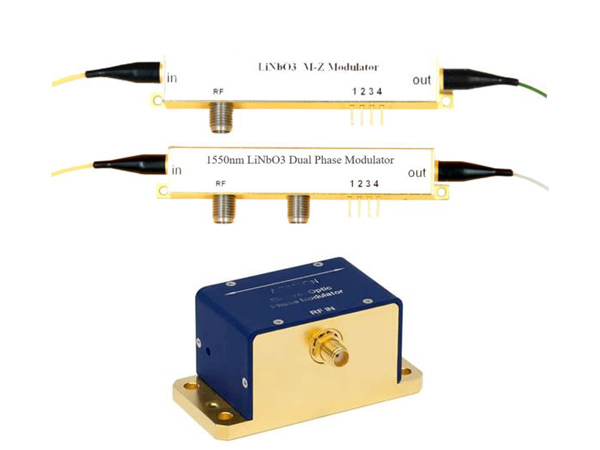
DUAL DRIVERS
Dual drivers allow simple or complex digital waveforms to be synthesized, converted to analog signals, and amplified to drive the AO device. This gives great flexibility; for example, it allows the driver to provide multiple programmable frequencies or to swap freely between multiple, complex, bespoke waveforms.
FREQUENCY AGILITY AND CONTROL
We offer Direct Digital Synthesizer (DDS) drivers that offer high stability and linearity, with fast switching time and high resolution. They are capable of creating arbitrary waveforms from a single, fixed-frequency reference clock, and thus are ideal for pulse shaping and special functions. DDS drivers can be run from a GUI or via driver commands in two modes: 1) random access, with digital words mapping to specific frequencies, and 2) chirped mode for continuous scanning in frequency increments. DDS drivers are also referred to as DFS (digital frequency synthesizer) drivers.
Our technical support team is available to advise on selection and optimization of RF drivers for specific applications, as well as customization of products for OEM integration.
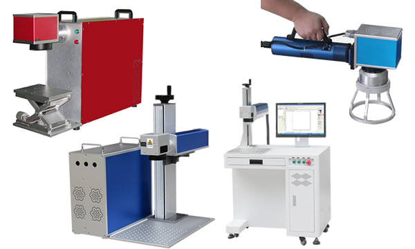
APPLICATIONS OF RF DRIVERS
Driving and control of acousto-optic devices, including modulators, deflectors, cavity dumpers, fiber-coupled modulators, frequency shifters, mode lockers, multi-channel modulators, pulse pickers, Q-switches, tunable filters.
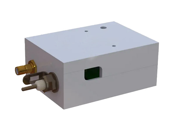
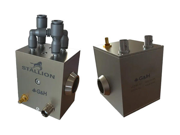
STQDP acousto-optic modulator driver is a completely new design, it is a low to medium power RF driver. This product is suitable for driving the acousto-optic modulator for short pulse lasers such as picosecond pulse selection (frequency reduction). Similarly, it can also be used in other RF fields. In fact, this is a completely independent innovation product. The most critical advantages of this product are cost performance, compact structure, stable RF output, strong anti-interference ability, and high reliability. Overall, it is an ideal drive source for acousto-optic modulator switches.
| Model | STQDPxxx-yyW-zzV-a |
| Output frequency | 200 MHz |
| Input to adjust the signal level | -D model: TTL, input impedance 75Ω -A model: ANALOG, 0-1V input, input impedance 51Ω -A5 model: ANALOG, 0-5V input, input impedance 51Ω -AD Accepts both TTL and ANALOG signals(0-1V). |
| RF rise/fall times | ≤10 ns |
| RF output power | potentiometer adjustable, highest power 5W |
| RF output impedance | 50Ω |
| Supply voltage | 12V, 15V Optional |
| Supply current | <1.5A,Varies according to rated power |
| Operating temperature conditions | Heat sink temperature should be between 10°~ 55°.The heat sink side of the drive must be fitted with a heat sink and this cooling surface or radiator must have 20W cooling capacity. |
| Storage temperature | -20°~ +85 |
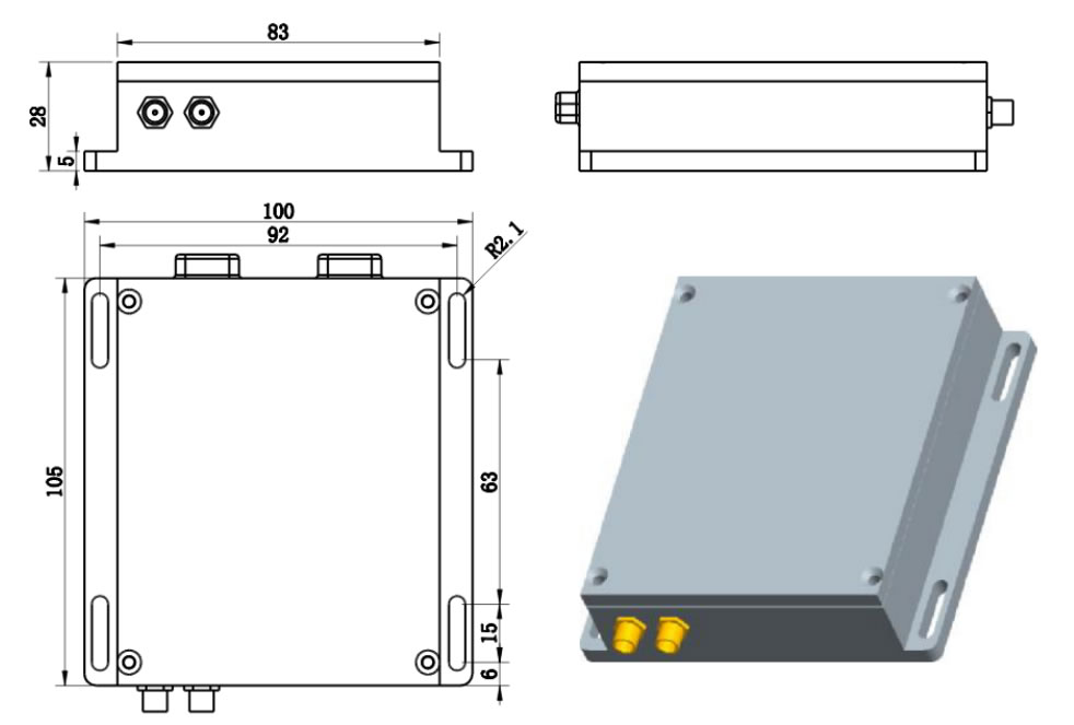
| Dimensions | 95*75*25mm (Smaller sizes is available: 49*68*22mm) |
Ordering Information: STQDPxxx-yyW-zzV-a
For example: STQDP200-2.5W-15V-D. This means that the output frequency 200MHz, rated output power 2.5W, Supply voltage 15V, and the factory default interface is digital interface.
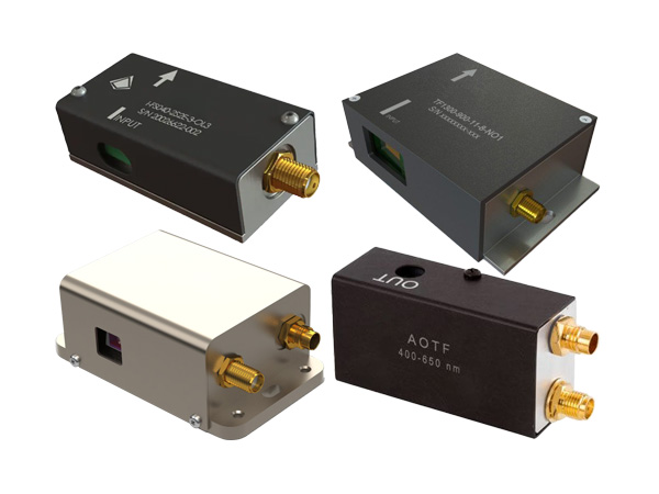
| Product | Compatible AO Device | Operating Frequency | Max RF Power | Key Feature |
| 97-05301-01 (1080HE-AD-1.0) | AOM, Frequency Shifter, Deflector | 20-80MHz | 1.4W | Compact, high efficiency RF driver, combined modulation |
| 64020-200-2ADMDFS-A | Deflector, Special Modulator, Tunable Filter | 20 - 200 MHz | 2.0 W | Programmable frequency; single channel DDS |
| 64020-250-1ADMDFS-A | Deflector, Special Modulator, Tunable Filter | 20 - 250 MHz | 1.0 W | Programmable frequency; single channel DDS |
| 97-02925-32 | Deflector, Tunable Filter | 20 - 160 MHz | 0.4 W | Programmable frequency; single channel DDS |
| 6000 Series | Deflector, Tunable Filter | 50-450 MHz | 15-20 W | Dual channel outputs, 2-axis scanning |
| 97-03926-12 | Deflector, Tunable Filter | 20 - 160 MHz | 3.2 W | Programmable frequency; 8 channel DDS |
| 97-02910-xx (2910 series) | Fiber-Q | 80-200 MHz | 2.5-3.0 W | Fixed single frequency; low power draw |
| 3307 series | Fiber-Q, Frequency Shifter | 80 - 350 MHz | 1-4 W | Fixed single frequency |
| 3910 series | Fiber-Q, Frequency Shifter, Modulator | 80 - 350 MHz | 0.5-8.0 W | Fixed single frequency |
| A35xxx-S-1/50-p4k7u | Fiber-Q, Frequency Shifter, Modulator | 40-300 MHz | 0.5-5.0 W | Fixed single frequency; analog & digital modulation |
| MHPXXX-YYADM-A1
Formerly N31xxx-yyADM |
Fiber-Q, Modulator | 24 - 260 MHz | 2-20 W | Fixed single frequency |
| MCX0XX-Y.YZC-MINx | Frequency Shifter, Modulator | 40-80 MHz | 0.5-2.5 W | Fixed single frequency; ultra-compact size |
| HP041-125ADG-A10 | Modulator | 40.68 MHZ | 125 W | Fixed single frequency; Ge AO devices |
| HP040-060-150ADG-A10-2X | Modulator | 40/60 MHz | 2 x75 W | Fixed dual frequencies; Dual channel Ge AO devices |
| Compact low power RF AOM and AO driver, QSQCxxx-yyDC-zz-aaV | Modulator, Q Switch | 24-110 MHz | 2-24 W | Fixed single frequency; compact, low power; fixed/variable pulse width |
| MQH0XX-YYDM-ZZZ | Modulator, Q Switch | 24-80 MHz | 25-100 W | Fixed single frequency; fixed/variable pulse width |
| MQH0XX-YYDM-ZZZ-2S | Q Switch | 24-80 MHz | 25-50 W per channel | Fixed single frequency; 2 channel; fixed/variable pulse width |
| SD020-200-5UC-4x1 | Tunable Filter | 20 - 200 MHz | 5.0 W | Programmable frequency; single or multi-channel DDS |
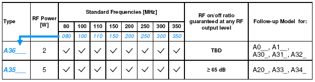
| Old RF Driver models below: | N31xxx-yyAM N31xxx-yyDM | MLPxxx-yAC MLPxxx-yAS MLPxxx-yDC MLPxxx-yDS (N21xxx-yAM N21xxx-yDM) | 1xxxAF-AINA-y HCR 1xxxAF-DINA-y HCR (A35xxx-S-1/50-p4k7u) | A36xxx |
| RF power | 2-20W | 0.4, 1 or 2W | 0~5W (Analogue) | 2W |
| RF frequency, MHz | 24-260 | 27-300 | 80, 100, 110, 150, 200, 250, 300, 350 | |
| Max. modulation frequency | <1/3 carrier frequency and <50MHz | |||
| Input modulation | Analogue or digital | Analogue and digital | ||
Description of N series drivers:
Description of A3 series drivers:
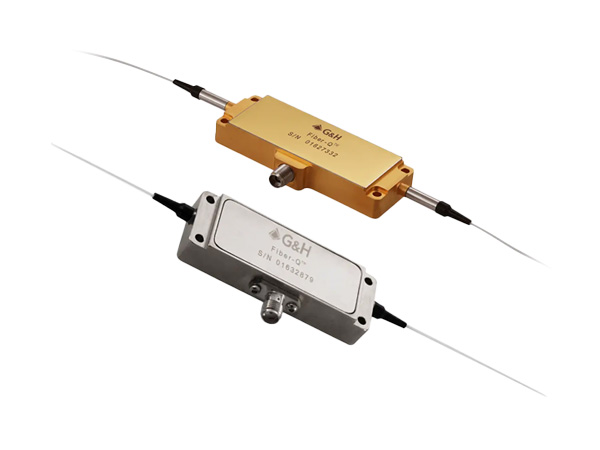
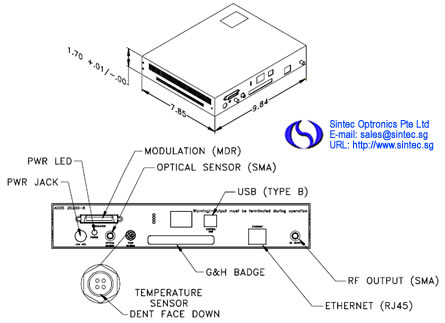
Each Fiber-Q acousto-optic modulator requires an RF driver to control the embedded acousto-optic crystal, as modulation of the beam depends upon the frequency and intensity of the applied RF signal.
The RF signal which generates the acousto-optic wave in the acousto-optic crystal can do so very precisely at a fixed or variable frequency, and is created using a transducer mated to the acousto-optic crystal and driven by the piezoelectric effect.
Analog, digital, and combined RF drivers are available for use with the Fiber-Q series. All are designed for dependable stability and high frequency operation, with compatible options for the full line of visible and NIR Fiber-Q products. The speed and stability of a modulator is limited by the stability and speed of the RF driver, and thus the two should be selected as a paired unit to optimize performance, features, and application-specific options.
The primary factors to consider when selecting an RF driver include the operating frequency, the required rise/fall time of the application, and whether analog or digital modulation is needed. RF power, duty cycle, stability, and variable vs fixed frequency are also relevant.
Drivers for the Fiber-Q series of modulators are designed for constant RF power output, fast modulation, and with conductive cooling via the baseplate. When tuned together with the modulator, they offer stable, dependable modulation to enable all-fiber laser systems.
| Model | Operating Frequency | RF Power | Key Features |
| 97-09210-18 | 80 MHz | 3.0 W | Analog |
| 97-09210-19 | 80 MHz | 3.0 W | Digital |
| A35080 | 80 MHz | 3.0 W | Analog/digital |
| A35110 | 110 MHz | 3.0 W | Analog/digital |
| 97-09210-14 | 150 MHz | 2.5 W | Analog |
| 97-09210-15 | 150 MHz | 2.5 W | Digital |
| A35150 | 150 MHz | 2.5 W | Analog/digital |
| 97-02910-04 | 200 MHz | 2.5 W | Analog |
| 97-02910-01 | 200 MHz | 2.5 W | Digital |
| A35200 | 200 MHz | 2.5 W | Analog/digital |
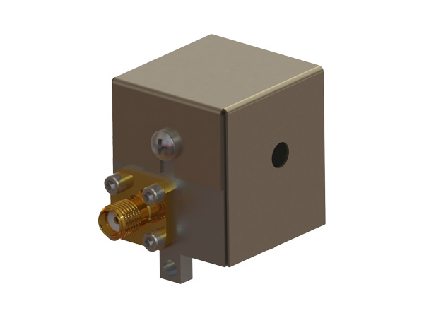
A digital frequency synthesizer OEM module with analog and digital modulation input and a 1 Watt RF output. The unit can be used to generate a frequency chirp. When specified as R64020-250-1ADMDFS-A, the unit delivered will be manufactured to be compliant with EU Directive 2002/95/EC for reduction of hazardous substance.
| PARAMETER | SPECIFICATION |
| Bandwidth: | 20 – 250 MHz typical |
| Clock Frequency: | 1000 MHz |
| Step Size: | < 1 Hz with 30 Bits input |
| Frequency Settling Time: | 310 ns Maximum |
| Power Out: | 1 watts typical |
| Harmonic Distortion: | 2nd:-20 dBc Maximum; 3rd: -15 dBc Maximum |
| Analog Modulation: | 0 to +1 volt Analog into 50 ohm, +1volt = Full RF power output. |
| Digital Modulation: | 1) TTL levels; 2) TTL Active High = Full RF output power; 3) TTL Active Low = Minimum RF output power; 4) No Signal = Full RF output power (pulled high internally) |
| Rise and Fall Time: | 20 ns |
| Extinction Ratio: Digital: | 30 dB Minimum |
| Analog: | 40 dB Minimum |
| Reference Out: | A reference signal from the un-modulated output of the synthesizer. +0 dBm nominal |
| Applied Power: | + 28 volts DC @ 1 amp Maximum + 3.3 volts DC @ 1 amp Maximum |
| MAXIMUM RATINGS: | |
| Ambient Temperature: | 400 C |
| RF Output: | No DC Feedback |
| INPUT / OUTPUT CONNECTIONS: | |
| +28v, +3.3V, and Gnd | Filtered Feedthru |
| Mod In | SMC Male |
| Reference Out | SMC Male |
| RF Output | SMA Female |
| "FREQUENCY SELECT" Control | TTL 30 bit binary word, Digital Modulation Input, Reset, and a Latch control input through the 37 pin D sub connector. |
| Dimension | 140x109x40.6mm |
| Outline Drawing | 53D3887 |
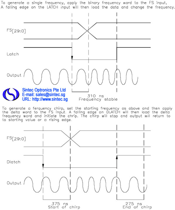
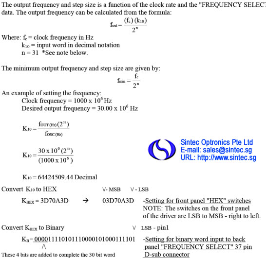
CONTROL WORD CALCULATIONS
The output frequency and step size is a function of the clock rate and the FREQUENCY SELECT (FS) data. The output frequency can be calculated from the formula:
FS[29:0] = Fout (231) / 1000 MHz
Where Fout is output frequency in MHz
The LATCH function (pin 16) is a TTL compatible input which is used to load new frequency information into the driver. Frequency data is loaded into the driver when the signal on the LATCH pin goes from HIGH to LOW (falling edge).
The DELTA FREQUENCY LATCH function (pin 36) is a TTL compatible input which is used to load new data frequency information into the driver. For Delta frequency word, the same calculation is used as the output frequency with negative values being entered in twos complement data is loaded on the falling edge.
Master RESET is a TTL active HIGH and resets the accumulator to zero, ie, no frequency output, when a TTL HIGH is applied to pin 17. This is pulled LOW via. a 1 K resistor.
A digital frequency synthesizer OEM module with analog and digital modulation input and a 2 Watt RF output. When specified as R64020-200-2ADMDFS-A, the unit delivered will be manufactured to be compliant with EU Directive 2002/95/EC for reduction of hazardous substance.
| PARAMETER | SPECIFICATION |
| Bandwidth: | 20 – 200 MHz typical |
| Clock Frequency: | 1000 MHz |
| Step Size: | < 1 Hz with 30 Bits input |
| Frequency Settling Time: | 250 ns Maximum |
| Power Out: | 2 watts typical |
| Harmonic Distortion: | 2nd:-20 dBc Maximum; 3rd: -15 dBc Maximum |
| Analog Modulation: | 0 to +1 volt Analog into 50 ohm, +1volt = Full RF power output. |
| Digital Modulation: | 1) TTL levels; 2) TTL Active High = Full RF output power; 3) TTL Active Low = Minimum RF output power; 4) No Signal = Full RF output power (pulled high internally) |
| Rise and Fall Time: | 20 ns |
| Extinction Ratio: Digital: | 30 dB Minimum |
| Analog: | 40 dB Minimum |
| Reference Out: | A reference signal from the un-modulated output of the synthesizer. +0 dBm nominal |
| Applied Power: | + 28 volts DC @ 1 amp Maximum + 3.3 volts DC @ 1 amp Maximum |
| MAXIMUM RATINGS: | |
| Ambient Temperature: | 400 C |
| RF Output: | No DC Feedback |
| Supply Voltage: | 30 volts DC; 3.5 volts DC |
| INPUT / OUTPUT CONNECTIONS: | |
| +28v, +3.3V, and Gnd | Filtered Feedthru |
| Mod In | SMC Male |
| Reference Out | SMC Male |
| RF Output | SMA Female |
| "FREQUENCY SELECT" Control | TTL 30 bit binary word, Digital Modulation Input, Reset, and a Latch control input through the 37 pin D sub connector. |
| Dimension | 140x109x40.6mm |
| Outline Drawing | 53D3887 |
CONTROL WORD CALCULATIONS
*Note: (1) This system only uses 30 bits to set the frequency output from the driver. The accumulator inside the chip is 31 bit, so use 231 in your calculations for precision. (2) The LATCH function (pin 16) is a TTL compatible input which is used to load new frequency information into the driver. Frequency data is loaded into the driver when the signal on the LATCH pin goes from HIGH to LOW (falling edge). (3) Master RESET is a TTL active HIGH and resets the accumulator to zero, ie, no frequency output, when a TTL HIGH is applied to pin 17. This is pulled LOW via. a 1 KΩ resistor.
| Part code | 160T1-1SNR-12-0.4J |
| Frequency specifications | |
| Frequency range | 20-160MHz |
| Frequency resolution (1) | 0.1Hz |
| Frequency stability | +/-2 ppm/deg C |
| Frequency preload time (2) | <10 us |
| Frequency toggle time (3) | <20ns |
| Amplitude Specifications | |
| RF output power (4) | 0.4W |
| RF output gain adjust (5) | 30dB |
| Modulation bandwidth (6) | >2MHz |
| Dynamic range (7) | >40dB |
| Intermodulation (8) | >40dB |
| Spurious | >30dBc |
| Signal to noise ratio (9) | >90dB |
| Interfaces | |
| RF output impedance | 50 Ohms |
| Amplitude modulation input level | 0-10V |
| FSK modulation input level | 3.3V |
| Blanking input level | 3.3V |
| Digital controls | ASCII |
| Sensor input | +/-3.3V |
| Power input,from DC supply | 12V@1A |
| Dimension | 165x132x25mm |
Remarks:
General Features
Specifications
| Part code | 160T2-8SAR-24-3.2B |
| Frequency specifications | |
| Frequency range | 20-160MHz |
| Frequency resolution (1) | 0.1Hz |
| Frequency stability | +/-2 ppm/deg C |
| Frequency preload time (2) | <8 us |
| Frequency toggle time (3) | <80ns |
| Amplitude Specifications | |
| RF output power | 3.2W |
| RF output power, per channel | 0.4W |
| Modulation bandwidth (4) | >2MHz |
| Dynamic range (5) | >35dB |
| Intermodulation (6) | >41dB |
| Spurious | >45dBc |
| Signal to noise ratio (7) | >75dB |
| Interfaces | |
| RF output impedance | 50 Ohms |
| Amplitude modulation input level | 0-10V |
| FSK modulation input level | 3.3V |
| Blanking input level | 3.3V |
| Digital controls | ASCII |
| Sensor input | +/-3.3V |
| Power input, from DC supply | 24V@2A |
| Dimension | 165x132x25mm |
Remarks:
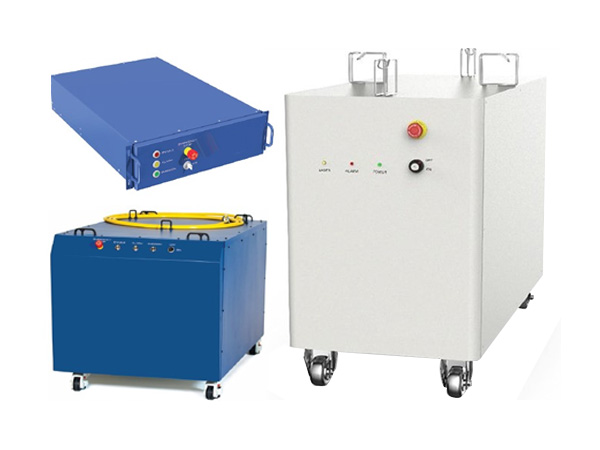
15 W Output – Configurable Operation
Our 15 W output RF driver provides up to two independent RF channels with a fast parallel interface as well as USB controllability.
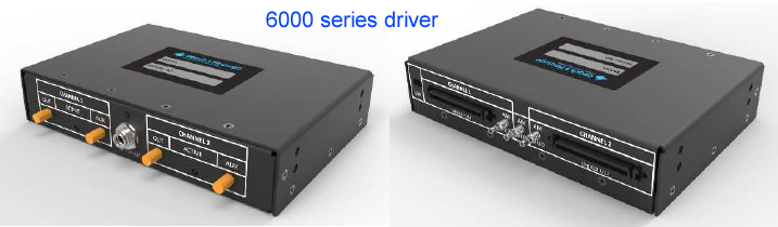
Ideally suited for controlling a two element phased array acousto-optic (AO) beam deflector (MUX mode), the driver can also be used to drive two single element AO beam deflectors for two dimensional scanning (Dual Channel mode). The 6000 driver has additional flexibility for controlling AO tunable filters (multi-tone mode). With its arbitrary waveform playback capability, multiple wavelengths can be simultaneously diffracted by tunable filters and multiple beam spots can be generated by beam deflectors.
Two independent 15 W RF amplifiers are housed in a compact form factor with a fast parallel frequency programming interface. Remote control over an included USB interface is also available with an intuitive command set and GUI. Dual amplitude and relative phase control inputs are included on the rear panel with the parallel interface connectors. Capabilities include dynamic frequency chirp control. An all digital option allows high speed programming of frequency, amplitude and phase. The default, power-on is stand-alone mode, not requiring PC control; connecting the USB connection enables a Host PC mode. A single channel version is also available.
The 6000 driver is available in three frequency bands, and each unit includes a monitor output that covers the entire 20-450 MHz frequency band. Driver functionality can be re-configured over the USB interface.
Key Features
Key Benefits
Applications
| Parameter | Min | Max | Units |
| Output frequency range: low band model mid band model high band model |
20 40 140 |
150 245 450 |
MHz |
| Rated RF output power (1)(9) | 15 | W | |
| RF power flatness (2) across frequency band, nominal power | +/-0.5 | dB | |
| 2nd harmonic distortion at rated RF output power | -25 | dBc | |
| Non-harmonic spurious free dynamic range | -50 | dBc | |
| Standard output waveform (3) | Sinusoid | n/a | |
| Independent RF outputs | 2 | n/a | |
| Number of programmable tones per output (4) | 5 | n/a | |
| Frequency resolution (5) | 1 | kHz | |
| Frequency stability, 15°C to 50°C ambient temperature | +/-0.5 | ppm | |
| Frequency settling time after latch signal assertion (6) | 200 | nS | |
| Frequency update rate (parallel interface) | 25 | MHz | |
| Amplitude control (analog input) range, each output channel (7) | 40 | dB | |
| Amplitude blanking | 80 | dB | |
| Relative phase control (analog input) range, relative (8) | 0 | +/-180 | Deg. |
| Amplitude/phase control modulation bandwidth | 25 | MHz | |
| DC voltage input range (9) | 24 | 28 | V |
| DC total system power | 100 | W | |
| Playback mode waveform file size (per output, 1 GHz clock) | 300 k | Samples | |
| Operating temperature range (ambient) | 15 | 50 | °C |
| Dimension | 7.27x5.98x1.65 | Inch |
All specifications at Tambient = 22 °C
Command Set (Host PC Mode via USB interface)
| Command | Action |
| Freq X, YYY | Sets output frequency YYY (MHz) on channel X (1 or 2) |
| Amp X, YY | Sets output power YY (00 – 99) on channel X (1 or 2) |
| Pha YYY | Sets relative phase to YYY (0 to 360 degrees) |
| Latch X | Latch command for channel X, latches the pre-loaded FTW |
| Soft on | Allows USB control of output power levels |
| Soft off | Reverts system to hardware mode, requires analog amplitude control |
Interface Description
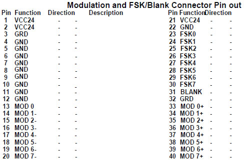
| Interface Definition | Connector | Levels | Input / Output Assignments |
| Parallel interface, Ch #1, #2 | MDR mini-D 68 pin (x2) | TTL | Frequency word [19:0], spares (5), latch In (1), trigger in (1), blank (1), sync (1), status out (1) |
| Amplitude modulation inputs | SMB (x2) | 0–1V | Ch #1, Ch #2 |
| Phase modulation input | SMB (x1) | 0–1V | Relative phase between channels |
| USB | USB mini-B | USB | USB 2.0 Interface (mass storage) |
| Main RF output | SMA (x2) | RF Output | Main RF output ports, per model |
| Aux RF output | SMA (x2) | Aux Output | Auxiliary RF output, 20-450 MHz |
| Main DC power input | 2mm power jack | 24–28 VDC | Main DC power input |
The 2910 Series RF driver provides up to 4 Watts output power. Various types cover a frequency range of 80 to 350MHz. The maximum RF output power is adjustable by an internal potentiometer. The driver is available in either analogue or digital modulation control. The analogue modulation voltage controls the output power from 0 to 100% of the adjusted maximum power. The digital modulation control signal can switch on and off the RF power.
The driver can be operated with modulation frequencies (analogue and digital) up to 25% of the carrier frequency and 50 MHz maximum at the higher carrier frequencies. Optimum EMC shielding and mechanical protection is achieved by an aluminium casing. The base plate serves for mounting and heat dissipation purposes.
Key Features:
Applications:
Technical Specifications:
| Supply voltage | +24V DC |
| Supply current | 600 mA (nominal) with Pout = 1.0 W 625 mA (nominal) with Pout = 1.5 W 775 mA (nominal) with Pout = 2.5 W 825 mA (nominal) with Pout = 3.0 W 900 mA (nominal) with Pout = 4.0 W 2700 mA (nominal) with Pout = 20 W* |
| Output impedance | 50 (nominal) |
| Maximum RF power (adjustable) | < 0.1 W … > Pout |
| Frequency accuracy | ± 0.1% |
| Harmonic distortion** | ≤ -20 dBc*** |
| Analogue modulation impedance Voltage range @50 RF ON/OFF ratio | 50 (nominal) 0 … +1 V ≥ 50 dB**** |
| Digital modulation Impedance Level RF ON / OFF ratio | 75 (nominal)***** Standard TTL ≥ 60 dB |
| RF output frequencies | 80, 110, 150, 200, 260 & 350 MHz |
| RF rise/fall times (Rise=10% to 90%) (Fall=90% to 10%) | 12 nsec @ 80 MHz 9 nsec @ 110 MHz 7 nsec @ 150 MHz 5 nsec @ 200 MHz 4 nsec @ 260 MHz 4 nsec @ 350 MHz |
Connectors
Cooling, Dimensions, Weight
| Cooling | Conduction Base plate should be attached to suitable heat sink capable of dissipating |
| 1.0 W - 1.5 W | 15 W |
| 2.5 W - 3.0 W | 20 W |
| 4.0 W | 22 W |
| Dimensions inches [mm] L x W x H | 4 x 1.12 x 3.15 [102 x 29 x 80] |
| Weight lbs [kg] | 0.53 [0.24] (nominal) |
Environmental Conditions
| Warn-up Time | 5 minutes (nominal) |
| Base Plate Temperature | 0C to +60C. For optimum output power stability constant base plate temperature should be provided |
| Storage Temperature | -25C to +85C (non condensing) |
Absolute Maximum Ratings
| Supply Voltage | +28 VDC |
| Analogue Modulation | -1.5 V to +1.5 V |
| Digital Modulation | -0.5 V to +2.75 V |
| Operating Temperature | +65C (base plate temperature) |
Quality Standards
Outline Drawing: Please click here for dimensions.
Variant List / Ordering Codes
Other Frequencies and customized versions available upon request.
Next Generation AO Modulator Driver
The 3910 series RF drivers offer a significant upgrade over our 2910 series while maintaining backwards compatibility.
The 2910 series RF driver has been a workhorse for powering AO modulator applications over the last decade. The line has received a complete makeover to further enhance the success of this signature driver. All of its functions have been improved and a few key features have been added while maintaining its affordable price.
The 3910 modulation input now allows the user to switch from three modulation schemes: Digital, Analog and Digital+Analog. This function will be standard on all models. The RF power has been doubled from 4Watts to 8Watts (at +28Vcc). The 3910 features more efficient power consumption than its predecessor. The Frequency range has been increased up to 500MHz, making it able to control any of the currently available AO modulator models. The rise time is <4ns at all power levels and frequencies >250MHz. Another new feature is the optional ability to synchronize the driver to an external clock reference. The 3910 RF driver offers more power, higher frequencies, faster rise times, more modulation choices, synchronization capabilities and the latest electronic components over the 2910 series driver while maintaining the same footprint and pricing.
Key Features
Key Benefits
Applications
| Parameter | Performance |
| Center frequency | 45 – 500 MHz fixed |
| RF output | 0.25 – 8.0 Watts adjustable (at +28 V) |
| Input voltage +Vcc | +24 to +28 V |
| 2nd harmonic level | < -20dBc |
| Output VSWR | 1.5:1 max |
| Output waveform | Sinusoidal |
| Rise / fall time | 4 nsec max (frequencies ≥ 250 MHz) |
| Contrast ratio | 50 dB min |
| Analog input voltage | 0 – 1 V |
| Analog input impedance | 50 Ohms |
| Digital input voltage | Standard TTL levels |
| Digital input impedance | 10 kOhms |
| Frequency stability | +/-1.5 ppm over temp |
| Frequency accuracy | +/-1% |
| Thermal management | Conduction cooled heat sink |
| Operating temperature range | 10°C to 60°C |
| Dimension | 4x1.12x3.31in (101.6x28.4x84mm) |
Model Code Generation:
Based on the different configurations, we split the 3910 driver part number into 12 categories as follows:
3910 - <3.0W, <100MHz, No heat sink, Internal Clock
3911 - <3.0W, 100-199MHz, No heat sink, Internal Clock
3912 - <3.0W, >199MHz, No heat sink, Internal Clock
3940 - >=3.0W, <100MHz, Heat sink, Internal Clock
3941 - >=3.0W, 100-199MHz, Heat sink, Internal Clock
3942 - >=3.0W, >199MHz, Heat sink, Internal Clock
3950 - <3.0W, <100MHz, No heat sink, External Clock
3951 - <3.0W, 100-199MHz, No heat sink, External Clock
3952 - <3.0W, >199MHz, No heat sink, External Clock
3960 - >=3.0W, <100MHz, Heat sink, External Clock
3961 - >=3.0W, 100-199MHz, Heat sink, External Clock
3962 - >=3.0W, >199MHz, Heat sink, External Clock
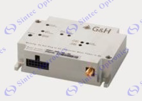
The A35xxx RF driver series provides up to 5 Watt output power. Various types cover a frequency range from 40 to 350 MHz.
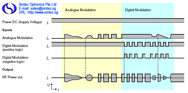
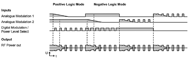
The maximum RF output power is adjustable by an internal potentiometer. The analogue modulation voltage controls the output power from 0 to 100% of the adjusted maximum power. Additionally to the analogue modulation voltage a digital modulation control signal can switch on and off the RF power. An operation scheme below (page 5) illustrates the interaction of the two modulation signals in detail. Both the analogue and digital modulation are characterized by extraordinary on/off ratios of at least 65dB. The driver can be operated with modulation frequencies (analogue and digital) up to 25% of the carrier frequency and 50 MHz maximum. Optimum EMC shielding and mechanical protection is achieved by an aluminium casing. The base plate serves for mounting as well as for heat dissipation.
Applications:
Technical Data:
+24 VDC
| Supply voltage | ||||
| Supply current | typ. 1.5 A @ 5 W RF output power | |||
| Output impedance | nom. 50W | |||
| Maximum RF output power (adjustable) * | > 5 W (+37 dBm) | |||
| Adjustment range | <0.1W …… >5W | |||
| Frequency accuracy | < ±25 ppm | |||
| Harmonics distortion* | < -26 dBc | |||
| Analogue modulation** | ||||
| Impedance | 50W | |||
| Voltage range @ 50W | 0 … +1 V | |||
| RF ON / OFF ratio | > 65 dB | |||
| Digital modulation** | ||||
| Impedance | 4.7kOhm (pull-up) | |||
| Level | High = ≥ 3V … 5V (=RF on)
Low = 0 … < 2V (=RF off) |
|||
| RF ON / OFF ratio | > 100 dB | |||
| RF output frequency*** [MHz] | 40 … <80 | 80 … <140 | 140 … <200 | 200 … 350 |
| Analogue modulation RF rise time / fall time (PRF: 10 … 90%) * | < 25 ns | < 15 ns | < 10 ns | < 8 ns |
| Digital modulation RF rise time / fall time (PRF: 10 … 90%) * | < 25 ns | < 15 ns | < 10 ns | < 8 ns |
Connectors, Dimensions, Weight, Cooling
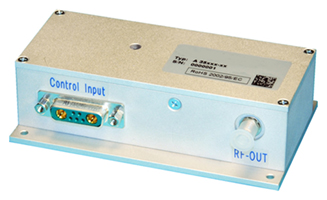
| RF output connector | SMA female |
| Control input connector | D-Sub 7W2 |
| Pins 1 and 2, inside linked | GND (case) |
| Pins 3 and 5, inside linked | +Vs (24 VDC) |
| Pin 4 | not connected |
| Pin A1 (coaxial) | Analogue modulation |
| Pin A2 (coaxial) | Digital modulation |
| Dimensions | 120 x 70 x 35 mm (LxWxH) |
| Weight | 360 grams |
| Cooling | Conduction, the base plate must be attached to a suitable heat sink. heat sink capable of dissipating 36 Watt. |
Environmental Conditions
| Warm up time | 10 minutes for optimum stability |
| Base plate temperature | +10°C … +60°C. For optimum output power stability constant base plate temperature should be provided. |
| Storage temperature | -20°C … +70°C, non condensing |
Absolute Maximum Ratings
| Supply voltage max. | +26 VDC |
| Analogue modulation | |
| Voltage range @ 0 … +1 V | -0.5 V … +1.1 V |
| Digital modulation | |
| Level | -0.5 V … +5.5 V |
| Maximum operating temperature | +65°C base plate temperature |
Quality Standards
| EU 2002/95/EC (RoHS) | compliant |
| EMC standards | VDE 0871-B FCC Rules Part 15-B |
| Thermal test | 2h @ 70°C passive |
| Burn-in test | 30 minutes @ maximum RF power output |
Control Input

Operation Scheme of Analogue and Digital Modulation
Variants List / Ordering Codes
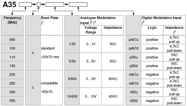
Other frequencies and customized versions are available on request.
Accessories
Connector Kit for AOM Driver Series A35xxx and A36xxx Part-No. 508A00169
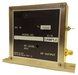
The MHPxxx-yyADM-A1 driver is a RF driver module with analog and digital modulation input and up to 20 Watts Output into a 50 Ohm load. The model number is described as follows:
| Output Frequency (xxx) | 24 MHz to 260 MHz ±0.01% quartz stabilized |
| Spurious Levels | -40 dBc maximum |
| Harmonic Distortion | -15 dBc maximum |
| Analog Input | 0-1 Volt into 50 Ohms (+ 1 Volt = Full RF power; 0 Volt = minimum RF power) |
| Digital Input | TTL Levels (TTL HIGH = FULL RF power; YYL LOW = minimum RF power) |
| Extinction Ratio | 40 dB minimum |
| RF Rise/ Fall Time | 30ns maximum, 20 ns typical, 10ns > 210MHz (PRF: 10 to 90%) |
| RF Output Power (yy) | 2 to 20 Watts nominal. maximum output power set by internal pot. |
| Output Impedance | 50 Ohms nominal |
| Supply Voltage | + 24 VDC + 0.5 Volt |
| Supply Current | 3 Amp maximum |
| Air Flow Across heat sink | 18 CFM at 25 oC |
| MAXIMUM RATINGS | |
| Supply Voltage | + 28 Volts |
| Power Output | No DC feedback allowed |
| Case Temperature | + 550C. |
| CONNECTORS & MECHANICAL | |
| RF Output Connector | BNC female |
| Modulation Input Connector | Feed Through Pin |
| Power Supply Connections | Vcc: Vcc feed through Pin; Return: Feed through Pin |
| Physical Size | 5.43" L x 2.42" H x 3.90" W |
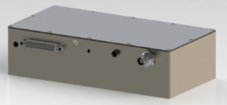
The HP041-125ADADG-A10 RF driver provides up to 125 Watt output power at 40.68 MHz signal frequency. The driver can be operated with modulation frequencies (analogue and digital) up to 1 MHz. An operation scheme illustrates the interaction of the two modulation signals in detail.
Water cooling parts made from copper ensures highest standards for corrosion protection. Optimum EMC shielding and mechanical protection is achieved by an aluminium casing and a conductive surface passivation.
This product conforms to the requirements of the European Union Directive 2011/65/EU of the European Parliament and of the Council on the Restriction of the Use of Certain Hazardous Substances in Electrical and Electronic Equipment.
Industrial (material processing): PCB via drilling; Marking and engraving; Light guide panel processing; Micro-perforation.
| Device: | AO Modulator |
| Supply voltage | +24 |
| Supply current | max. 12.5 @ 125 W F output power |
| Maximum RF output power (adjustable) *
Adjustment range |
> 15 W/mm2
< 1 … >125 Watt |
| Output impedance | nom. 50 Ω |
| Frequency accuracy | < ±30 ppm |
| RF ON/OFF ratio | > 50 dB |
| Analogue modulation Impedance Voltage range @ 50 Ω The voltage range corresponds to 0 to 100% of the potentiometer pre-adjusted maximum RF output power. |
600 Ω 0 … +10 |
| Digital modulation Impedance Level |
4.7 kΩ (pull-up) High=≥ 3 … 5 (= RF on); Low=0 … < 2 (=RF off) |
| Maximum modulation frequency (digital and analogue) | 1 [MHz] |
| RF output frequency | 40.68 [MHz] |
| Harmonics distortion * | < -30 [dBc] |
| Analogue modulation RF rise time / fall time(10 90%) * | < 80 [ns] |
| igital modulation F rise time / fall time(10 … 90%) * | < 80 [ns] |
* into 50 Ω load
| RF output connector | BNC female |
| Control connector | D-Sub 25-pole, female for pin assignment refer to section Control Connector |
| Power Supply Cords red (or yellow) black (or violet) |
2x750±50 mm H07-K 1.5 mm2 +Vs (24VDC) CGND (case ground) |
| Cooling Flow rate | Water cooling; Cooling block material: Copper, 2 x G 1/4’’ thread fitted with 6mm push in connectors; More than 1 litre/minute at less than 25˚C |
| Diemnsions [mm] | 200 x 100 x 52.5 (length x width x height) |
| Weight | 1470 grams |
D-Sub 25-pole, female, Pin assignment. Any signals refer to chassis ground (CGND ) unless denoted differently.
Pin1 RF ON status (out); Pin2 SWR fault indication (out); Pin3 Driver temperature fault indication (out); Pin4 Reset SWR fault / Init (in); Pin5 Interlock 2 fault indication (out); Pin6 Interlock 2 (in); Pin7 Interlock 1 (in); Pin8 Interlock 1 fault indication (out); Pin9 Driver temperature monitor (out); Pin10 Modulation Ground (MGND); Pin11 Analogue modulation 2 (ref. MGND); Pin12 Analogue modulation 1 (ref. MGND); Pin13 Power Level Select (ref. MGND); LOW →select Analogue Mod. 1; HIGH → select Analogue Mod. 2; Pin14…22 Chassis ground (CGND); Pin23…24 Modulation Ground (MGND); Pin25 not connected
 The HP040-060-150ADG-A10-2Xdriver provides up to 150 Watt combined output power and is designed to drive dual frequency germanium acousto-optic modulators. The driver can be operated with modulation frequencies (analogue and digital) up to 1 MHz for RF amplitude control and up to 5 MHz for drive frequency control. Water cooling parts made from copper ensures highest standards for corrosion protection. Optimum EMC shielding and mechanical protection is achieved by an aluminium casing and a conductive surface passivation. This product conforms to the requirements of the European Union Directive 2011/65/EU of the European Parliament and of the Council on the Restriction of the Use of Certain Hazardous Substances in Electrical and Electronic Equipment.
Industrial (material processing): PCB via drilling; Marking and engraving; Micro-perforation.
| Supply voltage | +24 VDC |
| Supply current | typ. 15A @ 150 W RF output power |
| Number of channels | 2 |
| Maximum RF output power (adjustable) * Adjustment range |
> 75 Watt W per channel < 1 … >75 Watt per channel |
| Output impedance | nom. 50 Ω |
| RF output frequency | 40MHz and 60MHz switchable (RF Signal phase shift between channels at 40 and 60MHz) |
| Frequency accuracy | < ±50 ppm |
| Frequency stability | < ±50 ppm |
| Extinction ratio | > 40 dB |
| Harmonics distortion* | < -26 dBc @ 75W per channel |
| Spurious level * | < -50 dBc |
| Analogue modulation Impedance Voltage range @ 50 Ω The voltage range corresponds to 0 to 100% of the potentiometer pre-adjusted maximum RF output power. |
600 Ω 0 … +10 (0…+5 option) |
| Digital / Frequency modulation Impedance Level |
4.7 kΩ (pull-up)
TTL compatible (V_ IL= 0.8V, V_IH = 2.0); Logic High = RF On / 40MHz; Logic Low = RF Off / 60MHz |
| Maximum modulation frequency (Amplitude – digital and analogue) (Drive frequency) |
1 MHz 5 MHz |
| Digital / Analogue modulation RF rise time / fall time (10 … 90%) |
< 100 ns |
* into 50 Ω load)
| Model | STBR-FF-XX-B1-FY | STBR-FF-XX-B2-FY | STBR-FF-XX-B3-FY |
| Output Frequency | XX MHz (compatible with the AO device) | ||
| Frequency control | Quartz crystal referenced phase locked loop | ||
| Frequency Accuracy | 0.015 | ||
| Harmonic Content (dBc) | <=-20 | ||
| Frequency Stability | 0.0015% minimum after 15 minute warmup | ||
| Output power | Power is optimised for peak efficiency with supplied AO device | ||
| Output protection | Power amplifiers used will tolerate an infinite VSWR without damage. Rated power is available only when a proper RF load is connected | ||
| Internal Pulse Generator | N/A | Pulse width: 100 to 500 nsec ± 10% adjustable, pulse generator with 5000 Hz to 100 KHz rep rate adjustable. Front panel switch for pulse/standby operation. | |
| Rise/Fall Time | To match AOM requirements | ||
| Modulation Type | Analog amplitude modulation | TTL compatible | Pulse modulation, pulse monitor output via front panel BNC connector |
| Modulation Rate | To match device requirements | ||
| Modulation Input | 50 ohml 0-1V | 330ohm; 0-5V | Internal or external trigger |
| Operating Power | 90-250 VAC, 50-60Hz, 55 W max | ||
| Enclosure | The unit will be packaged in a 190mm (7.5inch) wide by 90mm (4inch) high by 220,, (8,75inch) deep instrument case. The rear panel heat sink increases the depth to 240mm(9.75inches) maximum. The size is exclusive of connectors | ||
| Environmental | Nominal Lab conditions: Max temperature is +35 degC. The unit is not seals against moisture or condensing humidity | ||
RF drivers can generate RF signals at fixed or variable-frequencies. Specified waveforms could be produced by different modulated signals to meet the requirements of different acousto-optic components and determine how much an optical beam is modulated, deflected, or tuned. Our RF drivers are able to generate RF signal at 27.12MHz, 40.68MHz, 68MHz, 80MHz, 100MHz, 120MHz, 200MHz, 250MHz, 300MHz and even higher, with RF power up to 120W. A variety of operating modes are available including FPS, PPK, R05 and A05 (Analog). Acousto-optic variable-frequency series drive of frequency shifter, deflector and filter, can output RF signal with high precision and broad frequency range, and support digital control, analog control, etc. PC software is equipped with which users can set the frequency and power at will. The frequency sweeping and other functions can also be set (TA series). For high-speed frequency conversion applications, it is capable of fast frequency switching (TB series). These drivers are matched with our AOMs and other acousto-optic components.
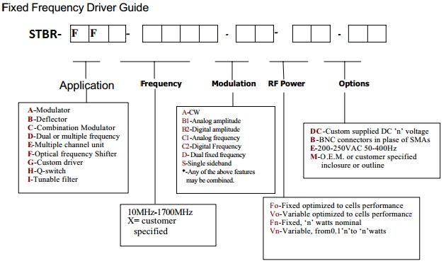
 1. Fixed-frequency series product number: STCT-CARD-as-f-vpt-bme-c
| Series(as) | RF(f) | Supply Power(v) | Output Power(p) | Cooling(t) | Chanel(b) | Mode(m) | Function(e) | RF Connector(c) |
| FA (Fixed-frequency series A) |
40.68 MHz 68 MHz 80 MHz |
15D (15 VDC) 24D (24 VDC) |
20 W 25 W |
C (Conduction-Cooled) |
1 | F (FPS) P (PPK) A (A05) R (R05) M (M05) |
C (Common) H (TTL_HIGH = RF on) L (TTL_HIGH = RF off) |
AF (SMA-F) |
| FD (Fixed-frequency series D) |
40.68 MHz 68 MHz 80 MHz 100 MHz 110 MHz 120 MHz ... |
12D (12 VDC) 15D (15 VDC) 24D (24 VDC) |
5W | C (Conduction-Cooled) A (Air-Cooled) W (Water-Cooled) |
1 | F (FPS) A (A05) D (Digital) |
||
| 20W | ||||||||
| 40W | ||||||||
| FB (Fixed-frequency series B) |
27.12 MHz 40.68 MHz 68 MHz 80 MHz |
24D (24 VDC) 28D (28 VDC) |
50W | C (Conduction-Cooled) A (Air-Cooled) W (Water-Cooled) |
1, 2 | F (FPS) A (A05) D (Digital) |
NF (BNC-F) |
|
| 100W | ||||||||
| FE (Fixed-frequency series E) |
200 MHz 250 MHz 300 MHz ... |
24D (24 VDC) |
2.5 W | C (Conduction-Cooled) |
1 | D (Digital) A (A05)* DA (Digital+Analog) |
AF (SMA-F) |
*Analog control voltage can be requested: A5: 0-5 V,A1: 0-1 V
Typical specifications:
| Working Frequency | Maximum RF Power | Rise/Fall time |
| 27.12 MHz | 100 W | <150 ns |
| 40.68/68/80 MHz | 15/20/25 W | <35 ns |
| 200/250 MHz | 2.5 W | <6 ns |
2. Variable-frequency series product number: STCT-CARD-as-f-vpt-bme-c
| Series(as) | RF(f) | Supply Power(v) | Output Power(p) | Cooling(t) | Chanel(b) | Mode(m) | Function(e) | RF Connector(c) |
| TA (Variable-frequency series A) |
60~120 MHz ... |
24D (24 VDC) |
0.5~4 W | C (Conduction-Cooled) |
1 | Programmable frequency | C (Common) ... |
AF (SMA-F) AM (SMA-M) |
| TB (Variable-frequency series B) |
70~120 MHz ... |
24D (24 VDC) |
0.5~4 W | C (Conduction-Cooled) |
1 | A (A05)* D (Digital) |
Px (channel) |
AF (SMA-F) |
| TE (Variable-frequency series E) |
70~120 MHz | 24D (24 VDC) |
0.5~4 W | C (Conduction-Cooled) |
1 | Voltage control 0~10V D (Digital) |
C (Common) ... |
AF (SMA-F) CF (SMC-F) |
*Analog control voltage can be requested: A10: 0-10 V,A5: 0-5 V,A1: 0-1 V
Typical specifications:
| Working Frequency | RF Power* | Working Mode*** | Switching Speed |
| 60~120 MHz | 4 W | Programmable frequency** | ~us |
| 70~120 MHz | 4 W | Voltage control 0~10 V, Digital** | ~50ns |
3. Detailed Specifications of Driver STCT-CARD-TA1-060-100-24D04C-1DA5H-AF
| Min. | Typ. | Max. | Unit | |
| Number of channels,RF output | 1 | Channel | ||
| Frequency Range CH1 | 60 | 100 | MHz | |
| Frequency stability | ±1 | Ppm/°C | ||
| Frequency accuracy | ±1 | kHz | ||
| Output Power1 CH1 | 2 | Watt | ||
| VSWR | 1.5/1 | |||
| Rise-time(10%-90%) | 2.5 | 6 | ns | |
| Fall-time(90%-10%) | 2.5 | 6 | ns | |
| Trigger frequency2 | DC | 1 | 10 | MHz |
| Extinction ratio | 45 | 50 | dB | |
| Harmonic Distortion | -20 | dBc | ||
| Output impedance | 50 | W | ||
| Analog input | 0 | 5 | V | |
| Digital control | Standard TTL (V_L<0.8V, V_H>2.0V) | |||
| Communication | RS232 (DB9) | |||
| Supply power | 24VDC, <0.8A | |||
| Operating temperature | +25 to +50°C | |||
4. Detailed Specifications of Driver STCT-CARD-TA1-040-24D04C-1DA5H-AF
| Min. | Typ. | Max. | Unit | |
| Number of channels,RF output | 1 | Channel | ||
| Frequency Range CH1 | 40 | MHz | ||
| Frequency stability | ±1 | Ppm/°C | ||
| Frequency accuracy | ±1 | kHz | ||
| Output Power1 CH1 | 1 | Watt | ||
| Output Power Ref | 0.5 | 1 | Vpp | |
| VSWR | 1.5/1 | |||
| Rise-time(10%-90%) | 2.5 | 6 | ns | |
| Fall-time(90%-10%) | 2.5 | 6 | ns | |
| Trigger frequency2 | DC | 1 | 10 | MHz |
| Extinction ratio | 45 | 50 | dB | |
| Harmonic Distortion | -20 | dBc | ||
| Output impedance | 50 | W | ||
| Analog input | 0 | 5 | V | |
| Digital control | Standard TTL (V_L<0.8V, V_H>2.0V) | |||
| Communication | RS232 (DB9) | |||
| Supply power | 24VDC, <0.8A | |||
| Operating temperature | +25 to +50°C | |||
The control mode can be changed according to customer needs:
Inferface definitions:
Dimensions:
A leading supplier and manufacturer of a wide range of photonics products such as lasers,laser parts & machines.
Office: 10 Bukit Batok Crescent #07-02 The Spire Singapore 658079
Tel: +65 63167112
Fax: +65 63167113
Whatsapp: +65 91904616